Your smartphone has approximately 110 meters (about 360 feet) of wiring. These wires connect the camera, speaker, screen, wifi antenna, GPS, battery, fingerprint sensor, dozens of microchips, and many more components into one device, enabling all components to work closely together. A football field’s length of wiring is precisely integrated into your smartphone, but where are these wires? Let’s slowly walk into the world of PCBs and uncover the mysteries within.
1. Introduction to PCB
PCB (Printed Circuit Board) is one of the essential components in the electronics industry, known in Chinese as 印制线路板 (Yìnzhì Xiànlù Bǎn) or simply 印制板 (Yìnzhì Bǎn). Almost every electronic device, from electronic watches and calculators to computers, communication electronics, and military weapon systems, requires a PCB for electrical interconnection between integrated circuits and other electronic components. The PCB provides the circuit structure and organization for all components to be installed on its surface. The wires in between connect each component to work together. So what is inside a printed circuit board, and how does it work?
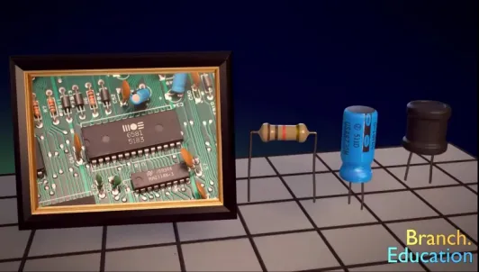
First, we need to understand the differences between electronic components, such as microchips, resistors, capacitors, connectors, and the PCB itself, as shown in Figure 1. These components are soldered onto the surface of the PCB. A PCB with electronic components installed is called a motherboard, while a PCB without any components is just a flat board. Some components, such as displays and cameras, are not directly installed on the PCB but are connected indirectly through connectors.
2. Structure of PCB
The PCB board consists of network interconnections on the surface of a substrate, mainly composed of substrate, copper foil, adhesive film, and solder mask ink.
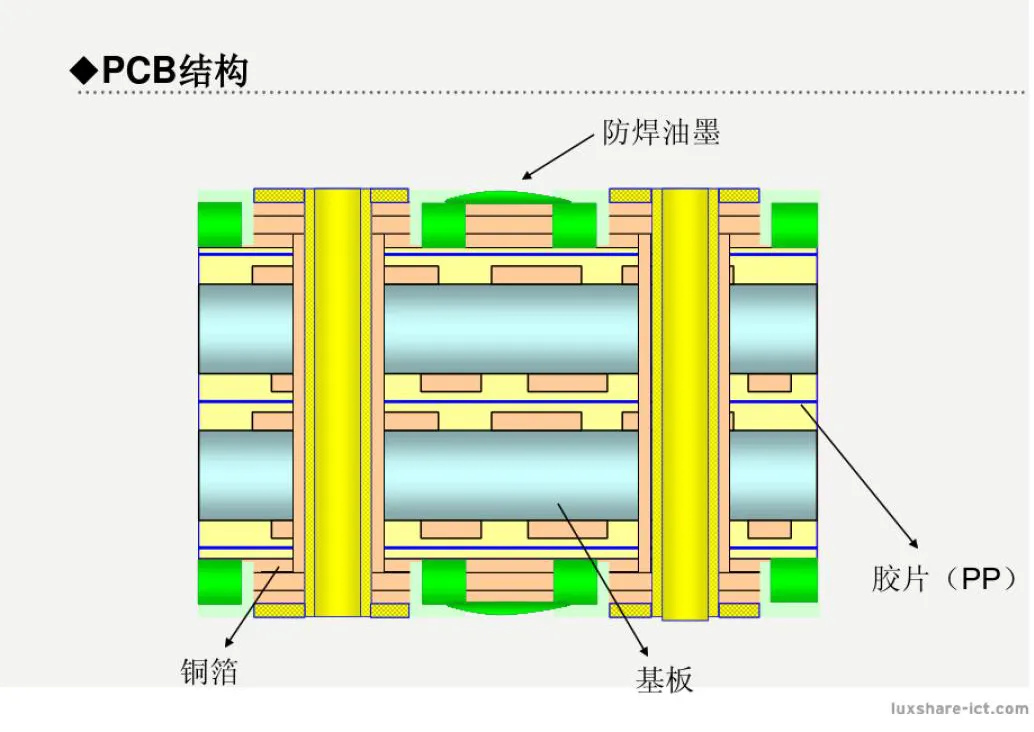
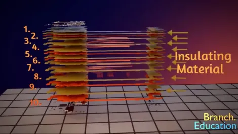
Multilayer board structure: Each conductive layer is made of copper, and each layer is separated by insulating fiberglass and epoxy resin. Most PCB boards have 2 to 10 layers of conductive layers. For example, the PCB board shown in Figure 3 has 10 conductive layers, each separated by an insulating layer (Insulating Material).
Each conductive layer is separated by insulating materials, so how do they interconnect? Vertical interconnect access, abbreviated as VIA, is responsible for performing the interconnection function. Figure 4 shows the process of VIA drilling, which requires pressing the PCB board between the aluminum cover plate and the backing plate of the drilling machine, then drilling with a drill bit. After drilling, a layer of copper is plated on the surface of the hole to enable connectivity between layers.
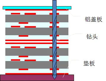
Figure 4: The process of VIA drilling.
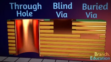
Figure 5: From left to right are through holes, blind holes, and buried holes.
There are three types of VIA: through holes, blind holes, and buried holes, as shown in Figure 5. Through holes refer to holes that go from the top layer to the bottom layer, blind holes refer to holes that go from the top or bottom layer to the middle layer, and buried holes connect internal layers. VIA can pass through multiple layers, and if they go through layers we do not want to connect, we need to remove the copper connected to the hole to ensure it does not contact the VIA.
3. Classification of PCB
The classification of PCB is shown in Figure 6a, while various PCB structures are illustrated in Figure 6b.
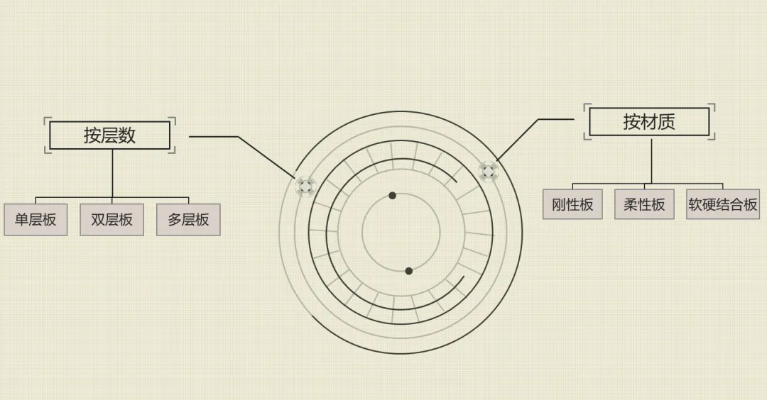
Figure 6a: Classification of PCB.
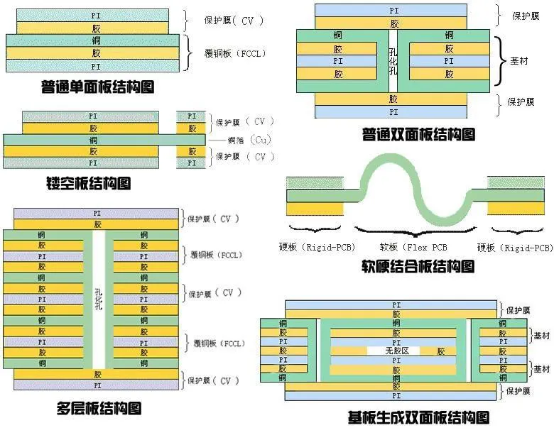
Figure 6b: Structures of various types of PCB.
4. PCB Manufacturing Process
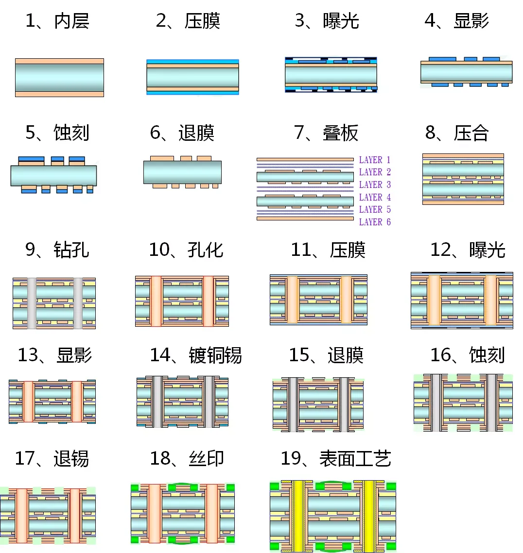
Figure 7: PCB manufacturing process.
The general manufacturing process of a PCB board is shown in Figure 7. It can be seen that the PCB process is quite complex, and many people have contributed their efforts and sweat to it. In recent years, people have focused on chip development, but who has considered how many components are behind a chip? From the smallest material to performance improvements of devices, and even to system design, it is the result of countless scientists and engineers working tirelessly day and night. The road of science is long and arduous, and we must not shy away from hard work and strive to make progress!
5. Applications of PCB
1. PCB in Mobile Phones
Nowadays, people cannot live without their mobile phones, and we achieve many functions through them. Do you know that the mobile phones we all use also contain PCBs?
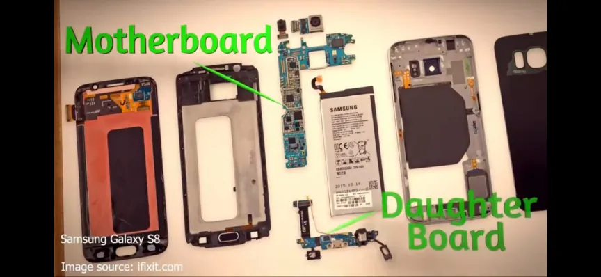
Each model of mobile phone has different shapes and specifications, thus having different printed circuit boards. Some phones separate the PCB at the top and bottom, with the larger one called the motherboard (Motherboard) and the smaller one called the daughter board (Daughter Board). For instance, Figure 8 shows the circuit board of the Samsung S8.
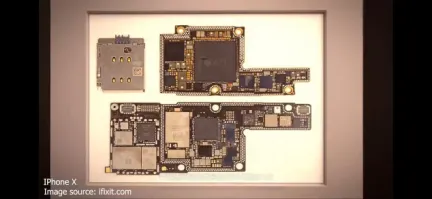
Some newer phones stack multiple PCBs together to save more space, and this type of PCB is both lightweight and small, weighing only a few grams. Figure 9 shows the PCB of the iPhone X. Engineers are constantly innovating to make various components as small as possible, with some even smaller than a flea. In contrast, older PCBs used components that took up a lot of space, installed on the surface and inside the board. The installation of older components required their legs to pass through a metal hole, so these older components are referred to as through-hole components.
2. PCB in Automobiles
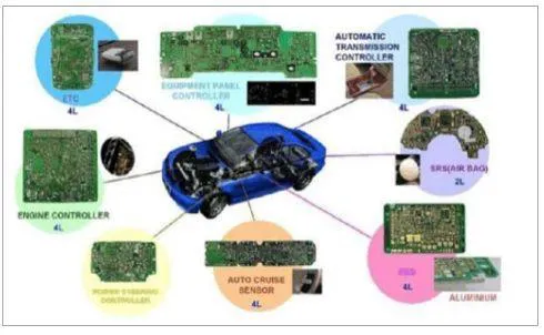
Figure 10: PCB in automobiles.

Image source from the internet; if there are any infringements, please contact us.
References:
[1] Xiao Ning. Research on the Filling Performance and Mechanism of EPE Series Copper Plating Inhibitors[D]. Harbin Institute of Technology, 2013.
[2] Tao Z, He W, Wang S, et al. Synergistic Effect of Different Additives on Microvia Filling in an Acidic Copper Plating Solution[J]. Journal of the Electrochemical Society, 2016, 163(8):D379-D384.
Source:Chengdu University of Electronic Science and Technology Graduate Student Science Popularization