1. Concept of PCB
PCB (Printed Circuit Board), known in Chinese as 印制电路板, is an important electronic component that serves as a support for electronic components and provides electrical connections between them. It is called a “printed” circuit board because it is made using electronic printing technology.
2. Role and Function of PCB in Various Electronic Devices
1. Pads: Provide mechanical support for the fixation and assembly of various electronic components such as integrated circuits.
2. Routing: Achieve wiring and electrical connections (signal transmission) between various electronic components such as integrated circuits, or provide electrical insulation. It provides the required electrical characteristics, such as characteristic impedance.
3. Green Oil and Silkscreen: Provide solder mask patterns for automatic assembly, and provide identification characters and graphics for component insertion, inspection, and maintenance.
3. Overview of PCB Technology Development
From 1903 to the present, the application and development of PCB assembly technology can be divided into three stages:
1. Through-Hole Technology (THT) Stage PCB
1. Role of metallized holes:
(1) Electrical interconnection – signal transmission
(2) Support for components – pin size limits the reduction of hole size
a. Rigidity of pins
b. Requirements for automated insertion
2. Ways to increase density:
(1) Reduce the size of component holes, but limited by the rigidity of component pins and insertion accuracy, hole diameter ≥ 0.8mm
(2) Reduce line width/spacing: 0.3mm—0.2mm—0.15mm—0.1mm
(3) Increase the number of layers: single-sided—double-sided—4 layers—6 layers—8 layers—10 layers—12 layers—64 layers
2. Surface Mount Technology (SMT) Stage PCB
1. Role of via holes: only serve the purpose of electrical interconnection, hole diameter can be as small as possible, and blocked holes are acceptable.
2. Main ways to increase density:
①. Via hole size drastically reduced: 0.8mm—0.5mm—0.4mm—0.3mm—0.25mm
②. Structural changes in vias:
a. Advantages of blind/buried vias: increase wiring density by more than 1/3, reduce PCB size or number of layers, improve reliability, enhance characteristic impedance control, and reduce crosstalk, noise, or distortion (due to shorter lines and smaller holes)
b. Hole-in-pad eliminates relay holes and connections
③. Thinning: double-sided boards: 1.6mm—1.0mm—0.8mm—0.5mm
④. PCB flatness:
a. Concept: The warpage of the PCB substrate and the coplanarity of the connection pads on the PCB surface.
b. PCB warpage is a comprehensive result of residual stress caused by heat and mechanical factors.
c. Surface coatings of connection pads: HASL, chemical Ni/Au, electroplated Ni/Au…
3. Chip Scale Package (CSP) Stage PCB
CSP has begun to undergo rapid transformation and development, driving PCB technology forward, and the PCB industry will move towards the laser and nano era.
4. PCB Surface Coating Technology
PCB surface coating technology refers to the solderable coating (plating) layer and protective layer for electrical connections, in addition to the solder mask coating (which also provides protection).
Classified by purpose:
1. For soldering: the surface of copper must have a coating layer for protection; otherwise, it easily oxidizes in the air.
2. For connectors: electroplated Ni/Au or chemical Ni/Au (hard gold, containing P and Co)
3. For wire bonding: wire bonding process
Hot air leveling (HASL or HAL) is a method of flattening PCBs that come out of molten Sn/Pb solder using hot air (230°C).
1. Basic requirements:
(1) Sn/Pb=63/37 (weight ratio)
(2) Coating thickness at least >3um
(3) Avoid the formation of non-solderable Cu3Sn, which occurs due to insufficient tin, such as when the Sn/Pb alloy coating is too thin, solder points consist of solderable Cu6Sn5– Cu4Sn3– Cu3Sn2—non-solderable Cu3Sn
2. Process flow: Remove resist—clean board surface—print solder mask and characters—clean—apply flux—hot air leveling—clean
3. Disadvantages:
a. The surface tension of lead-tin is too high, easily forming a turtle-back phenomenon.
b. The surface of the pads is uneven, which is not conducive to SMT soldering.
Chemical Ni/Au refers to the process of chemically plating Ni (thickness ≥3um) on the PCB connection pads, followed by plating a thin layer of gold (0.05-0.15um) or a thick layer of gold (0.3-0.5um). Due to the uniformity of the chemical plating layer and good coplanarity, it can provide multiple soldering capabilities, thus trending towards widespread application. The thin gold plating (0.05-0.1um) is to protect the solderability of Ni, while the thick gold plating (0.3-0.5um) is for wire bonding process requirements.
1. Role of Ni layer:
a. Acts as an isolation layer between Au and Cu, preventing diffusion between them, which causes the diffusion area to become loose.
b. Acts as a solderable plating layer, thickness at least >3um
2. Role of Au:
Au is the protective layer for Ni, thickness between 0.05-0.15, cannot be too thin, as gold has a high porosity, if too thin it cannot protect Ni well, causing Ni oxidation. Its thickness also cannot exceed 0.15um, as when Au exceeds 3% in solder points, solderability deteriorates.
Electroplated Ni/Au has a plating structure similar to chemical Ni/Au, but due to the use of electroplating, the uniformity of the plating layer is somewhat inferior.
5. PCB Design Output Production File Considerations
1. Layers that need to be output:
(1) Routing layers including top layer/bottom layer/middle routing layers;
(2) Silkscreen layers including top silkscreen/bottom silkscreen;
(3) Solder mask layers including top solder mask and bottom solder mask;
(4) Power layers including VCC layer and GND layer;
(5) Additionally, generate drilling files NCDrill.
2. If the power layer is set to Split/Mixed, then in the AddDocument window, select Routing in the Document item, and before each output of the photoplot file, use PourManager’s Plane Connect to copper pour the PCB diagram; if set to CAMPlane, then select Plane and when setting the Layer item, add Layer25 and select Pads and Vias in Layer25.
3. In the device settings window, change the Aperture value to 199 in Device Setup.
4. When setting each layer’s Layer, select BoardOutline.
5. When setting the silkscreen layer’s Layer, do not select PartType, select the top layer, bottom layer, and silkscreen layer’s Outline Text Line.
6. When setting the solder mask layer’s Layer, select vias to indicate that no solder mask is added on the vias. Generally, vias will be covered by the soldering layer.
6. Safety Marking Requirements
1. The safety marking of fuses must be complete, with six complete markings near the fuse, including fuse number, fusing characteristics, rated current value, explosion-proof characteristics, rated voltage value, and English warning markings. For example, F101 F3.15AH, 250Vac, “CAUTION: For Continued Protection Against Risk of Fire, Replace Only With Same Type and Rating of Fuse”. If there is no space on the PCB for the English warning marking, it can be placed in the product’s user manual.
2. High voltage warning symbols must be marked in the dangerous voltage area of the PCB, using a 40mil wide dashed line to separate the dangerous voltage area from the safe voltage area, and print high voltage warning symbols and “DANGER! HIGH VOLTAGE”.
3. The original and secondary edge isolation bands must be clearly marked, with dashed lines in the middle.
4. The safety markings on the PCB must be clear and complete.
7. PCB EMI Design
One of the most common issues in PCB design is EMI problems caused by signal lines crossing split grounds or power supplies. To avoid such EMI issues, the following introduces the normative steps for EMI design in PCB design.
1. Power handling of ICs
Ensure that each IC’s power PIN has a 0.1μF decoupling capacitor, and for BGA chips, it is required to have 0.1μF and 0.01μF capacitors at each of the four corners, totaling 8. Pay special attention to adding filter capacitors to power routing, such as VTT, etc. This not only affects stability but also has a significant impact on EMI. Generally, decoupling capacitors still need to follow the chip manufacturer’s requirements.
2. Handling of clock lines
1. It is recommended to route clock lines first.
2. For clock lines with a frequency greater than or equal to 66M, the number of vias per line should not exceed 2, with an average of no more than 1.5.
3. For clock lines with a frequency less than 66M, the number of vias per line should not exceed 3, with an average of no more than 2.5.
4. For clock lines longer than 12 inches, if the frequency is greater than 20M, the number of vias should not exceed 2.
5. If there are vias in the clock line, adjacent to the vias, add a bypass capacitor between the second layer (ground layer) and the third layer (power layer), as shown in Figure 2.5-1, to ensure that the high-frequency current loop of the reference layer (adjacent layer) is continuous after the clock line changes layers. The power layer where the bypass capacitor is located must be the power layer that the via passes through, and it should be as close to the via as possible, with a maximum distance of 300MIL between the bypass capacitor and the via.
6. All clock lines should not cross islands (splits). The following lists four situations where crossing islands is prohibited:
Clock, reset, signals above 100M, and some critical bus signals cannot cross splits, at least one complete plane must be present, preferably a GND plane.
Clock signals, high-speed signals, and sensitive signals are prohibited from crossing splits;
Differential signals must be balanced to ground, avoiding single lines crossing splits (preferably crossing splits vertically).
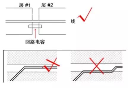
All high-frequency return paths of signals should be directly located beneath the signal lines on adjacent layers. Setting a solid layer beneath the signal can significantly reduce signal integrity and timing issues; this solid layer can provide a direct loop for the signal. When routing intersects with layer splits, a 0.01 uF loop capacitor should be used. As shown in the figure, when using a loop capacitor, it should be placed as close as possible to the intersection point of the signal line and the layer split.
6.1 Crossing islands occurs between power islands. In this case, the clock line is routed on the back of the fourth layer, and the third layer (power layer) has two power islands, and the routing on the fourth layer must cross these two islands.
6.2 Crossing islands occurs between power islands and ground islands. In this case, the clock line is routed on the back of the fourth layer, and there is a ground island in the middle of a power island on the third layer (power layer), and the routing on the fourth layer must cross these two islands.
6.3 Crossing islands occurs between ground islands and ground layers. In this case, the clock line is routed on the first layer, and there is a ground island in the middle of the second layer (ground layer), and the routing on the first layer must cross the ground island, effectively interrupting the ground line.
6.4 There is no copper pour under the clock line. If conditions restrict crossing islands, ensure that clock lines with a frequency greater than or equal to 66M do not cross islands; for clock lines with a frequency less than 66M, if they must cross islands, a decoupling capacitor must be added to form a mirrored path. For example, in the case of a clock line crossing between two power islands, place a 0.1UF capacitor near the crossing point of the clock line.
7. When faced with the choice between two vias and one crossing island, choose one crossing island.
8. Clock lines should be more than 500MIL away from the I/O side of the board and should not run parallel to I/O lines; if unavoidable, the distance between the clock line and the I/O line should be greater than 50MIL.
9. When clock lines are routed on the fourth layer, the reference layer (power plane) for the clock line should be as close as possible to the power plane supplying the clock; the fewer clock lines referenced to other power planes, the better. Additionally, for clock lines with a frequency greater than or equal to 66M, the reference power plane must be the 3.3V power plane.
10. When routing clock lines, the spacing between lines should be greater than 25MIL.
11. When routing clock lines, the incoming and outgoing lines should be as far apart as possible. Avoid routing methods similar to those shown in Figures A and C; if the clock line needs to change layers, avoid using the routing method shown in Figure E, and use the routing method shown in Figure F.
12. When connecting clock lines to devices such as BGA, if the clock line changes layers, avoid using the routing form shown in Figure G; do not route vias under the BGA, and it is best to use the routing form shown in Figure H.
13. Pay attention to each clock signal; do not overlook any clock, including the AUDIO CODEC’s AC_BITCLK. Especially note FS3-FS0; although they do not appear to be clocks by name, they actually run as clocks and should be noted.
14. Pull-up and pull-down resistors on the Clock Chip should be as close to the Clock Chip as possible.
3. Handling of I/O Ports
1. Each I/O port, including PS/2, USB, LPT, COM, SPEAK OUT, GAME, should be divided into a ground area, with the leftmost and rightmost connected to digital ground, with a width of no less than 200MIL or three vias; other areas should not be connected to digital ground.
2. If the COM2 port is pin-type, it should be as close to the I/O ground as possible.
3. EMI devices for I/O circuits should be as close to the I/O SHIELD as possible.
4. The power layer and ground layer at the I/O port should be separately islanded, and both the Bottom and TOP layers should have ground; signals should not cross islands (signal lines should be directly pulled out of the PORT, not routed long distances within the I/O PORT).
4. Some Explanations
1. Design engineers must strictly adhere to EMI design specifications; EMI engineers have the authority to check compliance. If non-compliance with EMI design specifications leads to EMI test failure, the responsibility lies with the design engineer.
2. EMI engineers are responsible for the design specifications and must provide solutions if EMI test failures occur despite strict adherence to EMI design specifications, and these solutions should be summarized in the EMI design specifications.
3. EMI engineers are responsible for EMI testing of each peripheral port and must not overlook any tests.
4. Each PCB design engineer has the right to suggest modifications to the design specifications and to question them. EMI engineers are responsible for answering these questions and incorporating suggestions into the design specifications after verification through experiments.
5. EMI engineers are responsible for reducing the cost of EMI design and minimizing the number of ferrite beads used.
8. ESD Suppression in PCB Design
PCB routing is a key element in ESD protection; reasonable PCB design can reduce unnecessary costs associated with fault checking and rework. In PCB design, transient voltage suppressor (TVS) diodes are used to suppress direct charge injection caused by ESD discharges, thus overcoming the electromagnetic interference (EMI) electromagnetic field effects generated by discharge currents is more important. This article will provide guidelines for optimizing ESD protection in PCB design.
1. Circuit Loop
Current enters the circuit loop through induction; these loops are closed and have varying magnetic flux. The magnitude of the current is proportional to the area of the loop. Larger loops contain more magnetic flux, thus inducing stronger currents in the circuit. Therefore, it is necessary to reduce the loop area.
The most common loop is formed by the power and ground lines. If possible, a multilayer PCB design with power and ground layers can be used. Multilayer circuit boards not only minimize the loop area between power and ground but also reduce the high-frequency EMI electromagnetic field generated by ESD pulses.
If multilayer circuit boards cannot be used, the lines for power and ground must be connected in a grid pattern. Grid connections can serve as power and ground layers, connecting printed lines of each layer through vias, with via connection intervals in each direction kept within 6 centimeters. Additionally, when routing, keep the printed lines for power and ground as close together as possible to reduce loop area.
Another method to reduce loop area and induced current is to minimize parallel paths between interconnected devices.
When long signal connection lines longer than 30 centimeters must be used, protective lines can be employed. A better approach is to place a ground layer near the signal line. Signal lines should be within 13mm of the protective line or ground line.
Cross the long signal lines (>30 centimeters) or power lines with their ground lines. The crossing connections must be arranged in a regular interval from top to bottom or left to right.
2. Length of Circuit Connections
Long signal lines can also act as antennas for receiving ESD pulse energy; using shorter signal lines can reduce the efficiency of signal lines as antennas for receiving ESD electromagnetic fields.
Try to place interconnected devices in adjacent positions to reduce the length of interconnecting printed lines.
3. Ground Charge Injection
Direct discharges of ESD to the ground layer can damage sensitive circuits. When using TVS diodes, one or more high-frequency bypass capacitors should also be used, placed between the power and ground of sensitive components. Bypass capacitors reduce charge injection and maintain the voltage difference between power and ground ports.
TVS diverts induced current, maintaining the potential difference of the TVS clamp voltage. TVS and capacitors should be placed as close as possible to the IC being protected, ensuring that the path from the TVS to ground and the length of the capacitor leads are minimized to reduce parasitic inductance effects.
9. Mark Point Design in PCB Production
1. The PCB must have a corresponding positioning mark point on the diagonal of the long edge of the board. For chips with a pin center distance of less than 0.65mm, there must be a corresponding chip positioning mark point on the diagonal of the long edge of the integrated circuit; if the PCB has components on both sides, then mark points must be added to both sides according to this rule.
2. The PCB edge must leave a 5mm process margin (minimum distance required for machine clamping of the PCB), and it must ensure that chips with a pin center distance of less than 0.65mm are more than 13mm (including process margin) from the board edge; the corners of the board should have a Ф5 round arc chamfer. The PCB should be designed in a panelized manner; considering the current degree of PCB warpage, the optimal panel length is about 200mm (maximum processing size: length 330mm; width 250mm), and it is best not to panel in the width direction to prevent bending during production. As shown in the figure:

3. Functions and Categories of Mark Points
Mark points, also known as reference points, provide common measurable points for all steps in the assembly process, ensuring that each device used in assembly can accurately locate the circuit pattern. Therefore, mark points are crucial for SMT production.
4. Recommended Mark Point Design Specifications
1) Shape: It is recommended that mark points be marked as solid circles with a diameter of R=1.0mm;
2) A complete mark point includes: a marking point (or feature point) and an open area.
3) Location: Mark points should be located at diagonal relative positions on the single board or panel and as far apart as possible; it is best to distribute them along the longest diagonal (as shown in the mark point location diagram).
4) To ensure the accuracy of the mounting requirements, SMT requires that each PCB must have at least one pair of mark points that meet design requirements, which can be recognized by SMT machines, and there must also be a single board mark (when panelized), while panel marks or combined marks only serve as auxiliary positioning.
5) When panelizing, the relative positions of the mark points on each single board must be the same. The position of any mark point on any single board in the panel must not be moved for any reason, leading to asymmetrical positions of the mark points on each single board.
6) All mark points on the PCB must meet the requirement that only pairs of two mark points appearing on the same diagonal are valid. Therefore, mark points must appear in pairs to be usable (as shown in the mark point location diagram).
7) The distance from the edge of the PCB to the edge of the mark point (open area) must be ≥5.0mm (minimum distance required for machine clamping of the PCB) (as shown in the mark point location diagram).
(Mark point location diagram)
8) Size
A. The minimum diameter of the mark point is 1.0mm, and the maximum diameter is 3.0mm. The size of the mark point on the same printed board should not vary by more than 25 microns;
B. It is particularly emphasized that all mark points on the same board number PCB must be consistent in size (including PCBs of the same board number produced by different manufacturers);
C. It is recommended that all mark points be uniformly set to a diameter of 1.0mm.
9) Open Area Requirements
There must be an area around the mark point marking that has no other circuit features or markings. The radius of the open area r≥2R, where R is the radius of the mark point, and r reaching 3R will improve machine recognition.
10) Material
Mark point markings can be bare copper or bare copper protected by a clear anti-oxidation coating. If solder mask is used, it should not cover the mark point or its open area.
11) The brightness of the mark points should remain consistent.
12) Flatness: The surface flatness of the mark point marking should be within 15 microns.
13) Contrast
A. The best recognition performance can be achieved when there is a high contrast between the mark point marking and the substrate material of the printed board.
B. The inner background of all mark points must be the same.
The following experiences in supplementing others are for reference:
Classification of Mark Points:
1) Mark points are used for optical positioning during solder paste printing and component placement. According to the role of mark points on the PCB, they can be divided into panel mark points, single board mark points, and local mark points (also known as device-level mark points).
2) There should be at least three mark points on the process edge of the panel and on single boards that do not require panelization, arranged in an L-shape, and the diagonal mark points should be asymmetrical about the center.
3) If both sides have mounted components, each side should have mark points.
4) Single boards that require panelization should have mark points if possible; if there is no place to place mark points, they can be omitted on the single board.
5) For QFPs with lead center distances ≤0.5 mm and BGAs with center distances ≤0.8 mm, local mark points should be set near the diagonal of the center point of the component for accurate positioning.
6) If several SOP components are relatively close (≤100mm) forming an array, they can be treated as a whole, and two local mark points should be designed at their diagonal positions.
Design instructions and size requirements:
1) The shape of the mark point is a solid circle with a diameter of 1mm, made of copper, with a tin-sprayed surface. Attention should be paid to flatness, with smooth and neat edges, and a color that is significantly different from the surrounding background color; the solder mask opening should be concentric with the mark point, with diameters of 3mm for panel and single board, and 1mm for local mark points.
2) For mark points on single boards, the center distance from the board edge should be no less than 5mm; for mark points on process edges, the center distance from the board edge should be no less than 3mm.
3) To ensure the recognition effect of printing and placement, there should be no pads, vias, test points, routing, or silkscreen markings within the mark point range, and they should not be cut by V-CUT grooves, which would prevent machine recognition.
4) To increase the contrast between the mark point and the substrate, copper foil can be laid under the mark point. The inner background of mark points on the same board should be consistent, meaning whether there is copper foil under the mark point should be the same.
5) Mark points on single boards and panels should be designed as components, while local mark points should be designed as part of the component package to facilitate accurate coordinate assignment for positioning.
Optical reference points in PCB design!
On PCBs with surface-mounted components, optical positioning points are usually required at the four corners of the PCB, generally three are sufficient. Common reference points mainly include three types: panel reference points, unit reference points, and local reference points.
Structure of Reference Points
(1) Panel reference points and unit reference points
Shape/Size: Solid circles with a diameter of 40mil. Solder mask opening: concentric circles with a size twice the diameter of the reference point. At the edge of 2mm diameter, a circular or octagonal copper wire is required as a protective ring. The optical positioning reference symbols on the same board must have the same inner background, meaning whether there is copper foil under the three reference symbols should be consistent.
(2) Local reference points
For QFPs with spacing ≤0.4mm and BGA, CSP, FC, etc., local reference points need to be placed.
Size/Shape: Solid circles with a diameter of 40mil.
Solder mask opening: treated as ordinary pads, the outer copper ring can be omitted.
Placement of Reference Points:
General Principle:
Single boards processed through SMT equipment must have reference points. The number of reference points on a single side should be ≥3.
When laying out a single side, reference points should only be placed on the component side. A5 I5 ^0 L- z1 m+ P For double-sided layouts, reference points should be placed on both sides. For double-sided reference points, except for mirrored panels, the positions of reference points on the front and back sides should be basically consistent. See the figure below.
(1) Placement of reference points for panelization
Panelization requires the placement of panel reference points and unit reference points.
Each of the panel reference points and unit reference points should be three in number, distributed in an L-shape along the edge of the board, as far apart as possible. The position requirements for panel reference points are shown in the figure A.
When using mirrored panels, the reference points on the auxiliary edge must meet the requirement of overlapping after flipping, as shown in figure B.
(2) Placement of reference points for unit boards
The number of reference points should be three, distributed in an L-shape along the edge of the board, with the distance between each reference point as far apart as possible. The distance from the reference points to the board edge must be greater than 5mm; if it cannot be ensured that all four edges meet this requirement, at least the conveying edge must meet the requirement.
10. Considerations for Clock PCB Routing Design
-
Layout
-
Clock crystals and related circuits should be placed in the central position of the PCB and have a good ground layer, rather than being close to I/O interfaces. Clock generation circuits should not be made into sub-cards or sub-boards; they must be placed on a separate clock board or carrier board.
As shown in the figure, it is best not to route in the area marked by the green box.
-
Only components related to the clock circuit should be routed in the PCB clock circuit area, avoiding the layout of other circuits. No other signal lines should be routed near or below the crystal: a ground plane should be used under the clock generation circuit and crystal. If other signals cross this ground plane, it violates the function of the image plane; if signals are allowed to cross this ground plane, there will be small ground loops that will affect the continuity of the ground plane, and these ground loops will cause problems at high frequencies.
-
For clock crystals and clock circuits, shielding measures can be employed;
-
If the clock casing is metal, ensure that copper is laid under the crystal in the PCB design, and ensure that this part has a good electrical connection with the complete ground plane (through multiple grounding points).
The benefit of laying ground under the clock crystal: the internal circuit of the crystal oscillator generates RF currents; if the crystal is in a metal casing, the DC power pin is relied upon as a DC voltage reference and the reference for the RF current loop inside the crystal. The ground plane releases transient currents generated by RF radiation from the casing. In summary, the metal casing acts as a single-ended antenna, and the nearest image layer, ground plane layer, and sometimes two or more layers serve as the coupling effect of RF currents to ground. Laying ground under the crystal is also beneficial for heat dissipation.
Laying ground under the clock circuit and crystal will provide an image plane, which can reduce common-mode currents generated by the related crystal and clock circuit, thus reducing RF radiation. The ground plane also absorbs differential-mode RF currents; this plane must be connected to the complete ground plane through multiple connections and requires multiple vias to provide low impedance. To enhance the effect of this ground plane, the clock generation circuit should be close to this ground plane.
-
SMT packaged crystals will radiate more RF energy than metal-cased crystals: because surface-mounted crystals are mostly plastic packaged, the RF currents inside the crystal will radiate into space and couple to other devices.
Shared clock routing
For fast rising edge signals and clock signals, a radial topology connection is better than using a single common driver source network in series; each routing should take termination measures according to its characteristic impedance.
Clock transmission line requirements and PCB layering
Clock routing principles: arrange a complete image plane layer adjacent to the clock routing layer, reduce the length of routing, and control impedance.
Incorrect cross-layer routing and impedance mismatches will lead to:
-
Routing using vias and jumps leads to incomplete image loops;
-
Surge voltages generated by voltage changes on signal pins of devices on the image plane;
-
If routing does not consider the 3W principle, different clock signals will cause crosstalk;
Clock signal routing
-
Clock lines must be routed on the inner layers of multilayer PCBs. If they must be routed on outer layers, they can only be routed as microstrip lines.
-
Routing on inner layers ensures a complete image plane, providing a low-impedance RF transmission path and generating magnetic flux to counteract the magnetic flux of their source transmission lines. The closer the source and return paths are, the better the demagnetization. Due to enhanced demagnetization capability, each complete plane image layer of high-density PCBs can provide 6-8dB of suppression.
-
The benefits of routing clock lines on multilayer boards: one or more layers can be dedicated to complete power and ground planes, designed as good decoupling systems, reducing the area of ground loops, lowering differential-mode radiation, reducing EMI, and lowering the impedance levels of signal and power return paths, maintaining consistency in the overall routing impedance, and reducing crosstalk between adjacent routing lines.
11. PCB Layer Stack Design
Before designing multilayer PCB circuit boards, designers need to first determine the structure of the circuit board based on the scale of the circuit, the size of the circuit board, and the requirements for electromagnetic compatibility (EMC), that is, deciding whether to use a 4-layer, 6-layer, or more layers of circuit board. After determining the number of layers, the placement of inner layers and how to distribute different signals on these layers must be determined. This is the issue of multilayer PCB stacking structure selection. The stacking structure is an important factor affecting the EMC performance of the PCB board and is also an important means of suppressing electromagnetic interference. This section will introduce the relevant content of multilayer PCB stacking structure. After determining the number of layers for power, ground, and signal layers, their relative arrangement positions are a topic that every PCB engineer cannot avoid.
General Principles for Layer Arrangement:
1. Determining the stacking structure of multilayer PCBs requires consideration of many factors. From a routing perspective, the more layers, the better for routing, but the cost and difficulty of manufacturing the board will also increase. For manufacturers, whether the stacking structure is symmetrical is a focus during PCB manufacturing, so the choice of the number of layers needs to consider various demands to achieve the best balance.
For experienced designers, after completing the preliminary layout of components, they will focus on analyzing the routing bottlenecks of the PCB. They will combine other EDA tools to analyze the routing density of the circuit board; then comprehensively consider the number and types of signals with special routing requirements, such as differential lines and sensitive signal lines, to determine the number of signal layers; then determine the number of inner layers based on the types of power, isolation, and anti-interference requirements. In this way, the total number of layers for the circuit board is basically determined.
2. The layer below the component surface (the second layer) should be a ground plane, providing a shielding layer for components and a reference plane for routing on the top layer; sensitive signal layers should be adjacent to an inner layer (internal power/ground layer), utilizing the large copper film of the inner layer to shield the signal layer. High-speed signal transmission layers in the circuit should be the signal middle layer, sandwiched between two inner layers. This way, the copper films of the two inner layers can provide electromagnetic shielding for high-speed signal transmission while effectively limiting the radiation of high-speed signals between the two inner layers, preventing external interference.
3. All signal layers should be as close to the ground plane as possible; 4. Try to avoid having two signal layers directly adjacent; adjacent signal layers are prone to crosstalk, leading to circuit function failure. Adding a ground plane between two signal layers can effectively avoid crosstalk. 5. The main power supply should be as close as possible to its corresponding ground; 6. Consider the symmetry of the lamination structure. 7. For motherboards, it is currently difficult to control parallel long-distance routing; for board-level operating frequencies above 50MHz (for frequencies below 50MHz, refer to and relax appropriately), the recommended layout principles are: the component surface and soldering surface should be complete ground planes (shielding); no adjacent parallel routing layers; all signal layers should be as close to the ground plane as possible; key signals should be adjacent to the ground layer and not cross split areas.
Note: When setting specific PCB layers, the above principles should be flexibly mastered. Based on understanding these principles, determine the arrangement of layers according to the actual needs of the single board, such as whether a key routing layer, power, and ground plane separation is needed, etc. Avoid rigidly applying these principles or fixating on one point.
8. Multiple ground inner layers can effectively reduce ground impedance. For example, A signal layer and B signal layer using separate ground planes can effectively reduce common-mode interference.
Common Stacking Structures:
4-Layer Board
Below is an example of a 4-layer board to illustrate how to optimize the arrangement and combination of various stacking structures.
For commonly used 4-layer boards, there are the following stacking methods (from top to bottom). (1) Signal_1 (Top), GND (Inner_1), POWER (Inner_2), Signal_2 (Bottom). (2) Signal_1 (Top), POWER (Inner_1), GND (Inner_2), Signal_2 (Bottom).
(3) POWER (Top), Signal_1 (Inner_1), GND (Inner_2), Signal_2 (Bottom). Clearly, scheme 3 lacks effective coupling between the power layer and ground layer and should not be adopted. So how should scheme 1 and scheme 2 be chosen? Generally, designers will choose scheme 1 as the structure for 4-layer boards. The reason for this choice is not that scheme 2 cannot be adopted, but because general PCB boards only place components on the top layer, so scheme 1 is more appropriate. However, when components need to be placed on both the top and bottom layers, and the dielectric thickness between the internal power layer and ground layer is large, leading to poor coupling, it is necessary to consider which layer has fewer signal lines. For scheme 1, the bottom layer has fewer signal lines, allowing for a large copper film to couple with the POWER layer; conversely, if components are mainly placed on the bottom layer, scheme 2 should be chosen. If a stacking structure as shown in Figure 11-1 is adopted, then the power layer and ground layer are already coupled, and considering the requirement for symmetry, scheme 1 is generally adopted.
6-Layer Board
After completing the analysis of the stacking structure for 4-layer boards, the following is an example of a 6-layer board combination method to illustrate the arrangement and optimization methods for 6-layer board stacking structures. (1) Signal_1 (Top), GND (Inner_1), Signal_2 (Inner_2), Signal_3 (Inner_3), POWER (Inner_4), Signal_4 (Bottom). Scheme 1 adopts 4 signal layers and 2 internal power/ground layers, which is beneficial for routing work between components, but this scheme also has obvious drawbacks, reflected in the following two aspects. ① The power layer and ground layer are separated too far, lacking sufficient coupling. ② Signal layer Signal_2 (Inner_2) and Signal_3 (Inner_3) are directly adjacent, leading to poor signal isolation and easy crosstalk.
(2) Signal_1 (Top), Signal_2 (Inner_1), POWER (Inner_2), GND (Inner_3), Signal_3 (Inner_4), Signal_4 (Bottom). Compared to scheme 1, scheme 2 has sufficient coupling between the power layer and ground layer, providing certain advantages, but the issues of direct adjacency between Signal_1 (Top) and Signal_2 (Inner_1) as well as between Signal_3 (Inner_4) and Signal_4 (Bottom) have not been resolved, leading to poor signal isolation and potential crosstalk.
(3) Signal_1 (Top), GND (Inner_1), Signal_2 (Inner_2), POWER (Inner_3), GND (Inner_4), Signal_3 (Bottom). Compared to schemes 1 and 2, scheme 3 reduces one signal layer and adds one inner power layer. Although the available routing layers are reduced, this scheme resolves the common defects of schemes 1 and 2. ① The power layer and ground layer are closely coupled. ② Each signal layer is directly adjacent to an inner layer, effectively isolating it from other signal layers, reducing the likelihood of crosstalk. ③ Signal_2 (Inner_2) is adjacent to the two inner layers GND (Inner_1) and POWER (Inner_3), which can be used for transmitting high-speed signals. The two inner layers can effectively shield external interference from the Signal_2 (Inner_2) layer and vice versa.
In summary, scheme 3 is clearly the most optimized one, and scheme 3 is also a commonly used stacking structure for 6-layer boards. Through the analysis of the above two examples, readers should have a certain understanding of stacking structures, but sometimes a single scheme may not meet all requirements, which requires consideration of the priority of various design principles. Unfortunately, due to the close relationship between the design of the board layers and the characteristics of the actual circuit, the anti-interference performance and design focus of different circuits vary, so in fact, these principles do not have a fixed priority for reference. However, it can be determined that design principle 2 (the internal power layer and ground layer should be closely coupled) must be satisfied first during design, and if high-speed signals need to be transmitted in the circuit, then design principle 3 (the high-speed signal transmission layer in the circuit should be the signal middle layer, sandwiched between two inner layers) must also be satisfied.
10-Layer Board
The typical design of a 10-layer PCB generally follows the wiring order of TOP–GND—signal layer—power layer—GND—signal layer—power layer—signal layer—GND—BOTTOM. This wiring order is not necessarily fixed, but there are some standards and principles to constrain it: for example, the adjacent layers of the top and bottom should be GND to ensure the EMC characteristics of the single board; each signal layer should preferably use a GND layer as a reference plane; the entire single board should use a complete copper foil for the power supply; signals that are susceptible to interference, high-speed, and along transitions should preferably be routed on inner layers, etc.
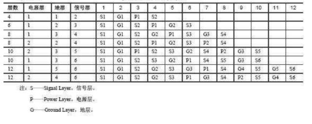
The table below provides reference schemes for multilayer board stacking structures for reference.
Case Study of Improving PCB Design Stacking Structure (From Jinbai Technology)
Problem Point
The product has 8 sets of network ports and optical ports. During testing, it was found that the signal debugging between the eighth optical port and chip was not working, leading to the eighth optical port being non-functional, while the other 7 optical ports communicated normally.
1. Confirmation of Problem Point
According to the information provided by the client, it was confirmed that the differential impedance lines between L6 layer optical port 8 and chip 8 were not working.
2. Client Provided Stacking and Design Requirements
Improvement Measures
Analysis of factors affecting impedance signals:
Line diagram analysis: The client’s L56 layer impedance design is relatively special, with L6 layer impedance referencing L5/L7 layers, and L5 layer impedance referencing L4/L6 layers, where L5/L6 layers are mutual reference layers, and there is no ground shielding in between. The long line between optical port 8 and chip 8 on L6 layer has a long parallel signal line (about 30% of the length), which easily causes mutual interference, thus affecting the accuracy of impedance. The design of the impedance line shielding layer is incomplete, also causing discontinuity in impedance. Other 7 groups have similar issues, but relatively mild. The L56 layer has a special design (all signal layers, with parallel differential impedance design, and no reference ground layer designed between adjacent impedance layers), and the client did not fully consider the interference caused by routing on adjacent layers, leading to debugging issues.
After communicating with the client to optimize the stacking, the structures of layers L45, L56, and L67 were adjusted, with the dielectric layer thickness changed from 20.87mil, 6mil, 13mil to 5.12mil, 22.44mil, 5.12mil, bringing the reference ground layer distance between L4 and L7 closer, and increasing the distance of the L56 layer’s mutually referenced and insufficiently shielded line layer to reduce interference. The optimized stacking structure:
Impedance Matching After Optimization:
Improvement Effect
By adjusting the stacking structure and increasing the distance between adjacent signal layers on L56, the system fault issues caused by crosstalk were resolved.