Previously, we discussed various aspects of crosstalk, including its sources, formation, types, simulation, and testing methods. We also introduced some methods to reduce crosstalk, one of which is to protect important signal networks with ground networks. This additional ground network is commonly referred to as a guard trace, as shown in the figure below:
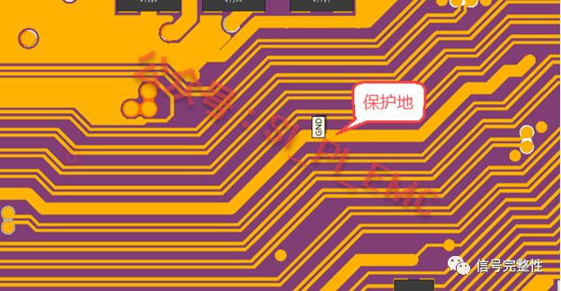
Can this ground network GND really protect the signal network? Especially for the type of ground network shown in the figure above (without ground vias). In this article, we will discuss whether this ground network is truly necessary.
At the end of the article, we will provide a summary based on experimental and simulation conclusions.
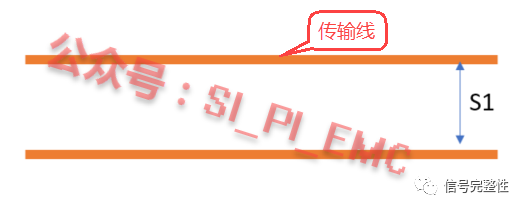
Typically, if there is no guard ground design or isolation ground structure, it is shown in the figure below:
If a guard ground structure is added, it is shown in the figure below:
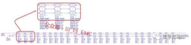
For such complex issues, we can conduct simulation analysis through modeling. By establishing a simple model in ADS, we can qualitatively study it. Different structures can be modeled as follows.
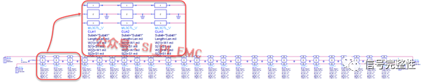
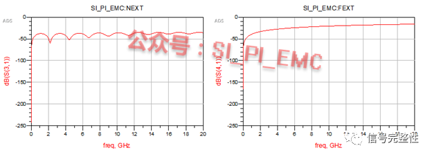
When considering the guard ground, the guard trace is generally placed 1W (line width) or 1H (distance from signal to reference layer) away from the protected signal network, modeled as shown in the figure below:
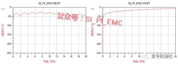
The simulation results for near-end and far-end crosstalk are shown in the figure below:
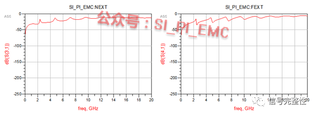
If the guard ground is grounded at one-tenth of the wavelength (equivalent to a ground via), its structure is shown in the figure below:
The simulation results for near-end and far-end crosstalk are shown in the figure below:
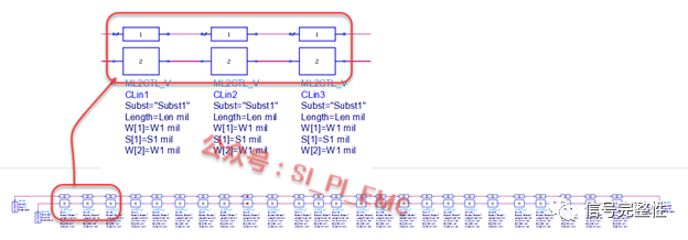
If a guard trace is added but not connected to the ground, its structure is shown in the figure below:

The simulation results for near-end and far-end crosstalk are shown in the figure below:
In the absence of a guard ground, the spacing between the two signal networks will be relatively large, modeled as shown in the figure below:
The simulation results for near-end and far-end crosstalk are shown in the figure below:

When we place the four simulation results together, the comparative results are shown in the figure below. dB(S(3,1)) indicates the result without a guard ground, dB(Guardtrace_2..S(3,1)) indicates the result with a guard trace but without grounding in between, dB(Guardtrace_2gnd..S(3,1)) indicates the result with a guard ground, grounded at one-tenth of the wavelength, and dB(Guardtrace_open..S(3,1)) indicates the result without grounding (open circuit):
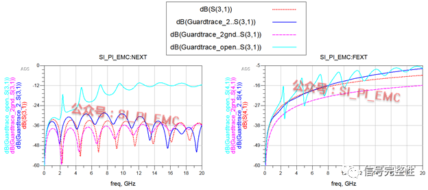
From the comparative results, we can see:
1. When the copper plane is retained but not connected to GND, crosstalk is the highest.
2. When the copper plane is retained and connected to GND, i.e., the “guard ground” is retained, but if ground vias are not placed at one-tenth of the wavelength (GND placed at 1/10 spacing), crosstalk will still be relatively high.
3. When the copper plane is retained and connected to GND, i.e., the “guard ground” is retained, and ground vias are placed at one-tenth of the wavelength, crosstalk will be lower, yielding the best results.
4. If there is enough space, removing the copper plane, i.e., not adding a guard ground, will also yield relatively good results, but it will be slightly worse than placing ground vias at one-tenth of the wavelength.
The above conclusions are obtained from limited experiments and are part of recent research on crosstalk. There are additional results that will be shared once the verification board is completed, so these conclusions are for reference only. If anyone is interested, they can conduct further analysis and research.
Book Recommendations:

Click “Read Original” to quickly access the details.