A Detailed Analysis of PCB Manufacturing Processes with Illustrations.
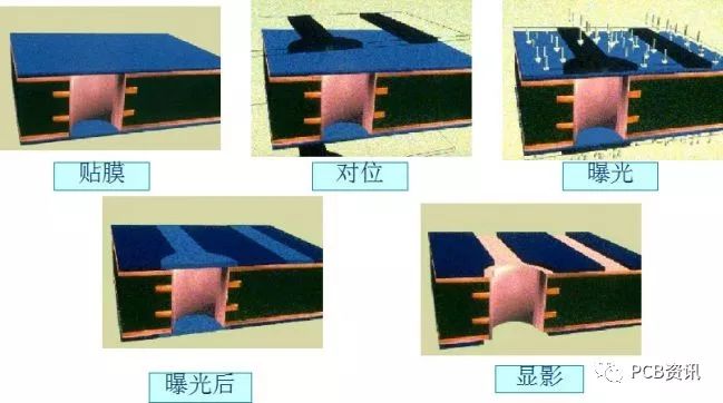
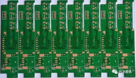
1. Cutting (CUT) Cutting is the process of slicing the raw copper-clad board into boards that can be made on the production line. First, let’s understand a few concepts: (1) UNIT: A UNIT refers to the unit graphics designed by PCB design engineers. (2) SET: A SET refers to a complete graphic formed by combining multiple UNITS for reasons such as improving production efficiency and convenience. This is what we often call a panel, which includes unit graphics, process edges, etc. (3) PANEL: A PANEL refers to a board produced by PCB manufacturers that combines multiple SETs together with tool board edges to improve efficiency and facilitate production. 2. Inner Dry Film (INNER DRY FILM) The inner dry film is the process of transferring the inner circuit graphics onto the PCB board. In PCB manufacturing, we often mention the concept of graphic transfer, as the creation of conductive graphics is fundamental to PCB production. Therefore, the graphic transfer process is very significant for PCB manufacturing. The inner dry film includes multiple processes such as inner film attachment, exposure development, and inner etching. The inner film attachment is the process of attaching a special photosensitive film to the surface of the copper board, known as dry film. This film solidifies upon exposure to light, forming a protective layer on the board. Exposure development involves exposing the board with the film attached; the parts exposed to light solidify, while the unexposed parts remain dry film. After development, the unexposed dry film is removed, and the board with the solidified protective film is etched. After stripping, the inner circuit graphics are transferred onto the board. The entire process flow is shown in the figure below.
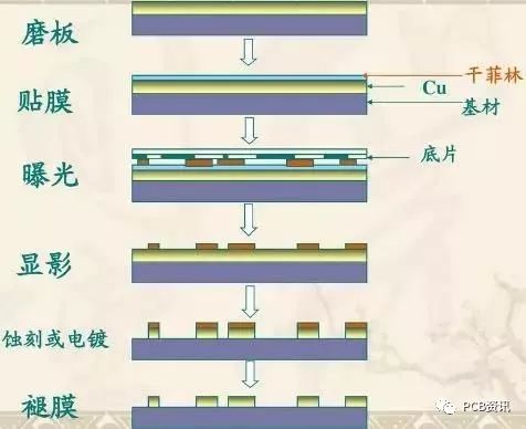 For designers, the main considerations are the minimum line width, spacing control, and uniformity of routing. If the spacing is too small, it can cause film trapping, leading to short circuits. If the line width is too small, the adhesion of the film is insufficient, causing open circuits. Therefore, the safety spacing during circuit design (including line-to-line, line-to-pad, pad-to-pad, line-to-copper surface, etc.) must consider the safety spacing during production. (1) Pre-treatment: Board Grinding The main purpose of board grinding is to address surface cleanliness and roughness issues. It removes oxidation and increases the roughness of the copper surface, facilitating film adhesion to the copper surface.
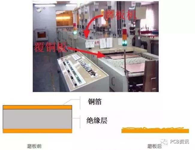 (2) Film Attachment The treated substrate is attached with dry film or wet film through hot pressing or coating, facilitating subsequent exposure production.
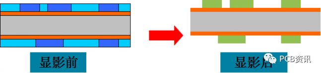
(3) Exposure The film is aligned with the substrate with the dry film pressed on it, and the graphic is transferred onto the photosensitive dry film using ultraviolet light exposure.
Physical Image of the Negative Film
(2) Film Attachment The treated substrate is attached with dry film or wet film through hot pressing or coating, facilitating subsequent exposure production.
(3) Exposure The film is aligned with the substrate with the dry film pressed on it, and the graphic is transferred onto the photosensitive dry film using ultraviolet light exposure.
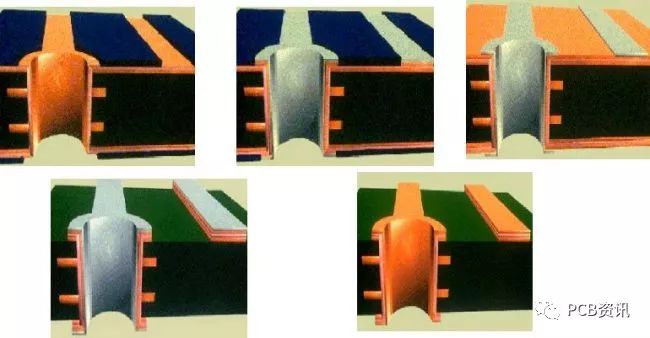
Physical Image of the Negative Film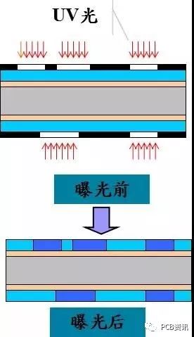 (4) Development The developing solution (sodium carbonate) dissolves and washes away the unexposed dry/wet film, while retaining the exposed parts.
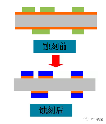
(5) Etching After the unexposed dry/wet film is removed by the developing solution, the exposed copper surface is dissolved and corroded by acidic copper chloride, resulting in the desired circuit.
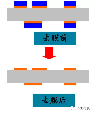
(6) Stripping The protective dry film is stripped off the exposed copper surface using sodium hydroxide solution, revealing the circuit graphics.
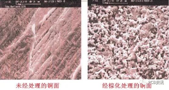
3. Brown Oxidation The purpose is to create microscopic roughness and an organic metal layer on the inner copper surface to enhance interlayer adhesion.
The process principle involves generating a uniform organic metal layer structure with good adhesion properties through chemical treatment, controlling the roughening of the inner copper layer surface before bonding with the prepreg to enhance bonding strength after pressing.
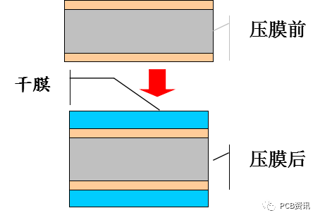
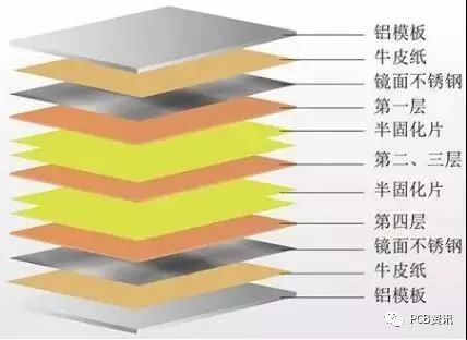
4. Lamination Lamination is the process of bonding various layers of circuits into a whole using the adhesive properties of prepreg. This bonding occurs through mutual diffusion and penetration between large molecules at the interface, resulting in interweaving, while pressing the discrete multilayer boards with prepreg to achieve the required number of layers and thickness. In actual operation, copper foil, bonding sheets (prepreg), inner layers, stainless steel, isolation boards, kraft paper, outer steel plates, and other materials are stacked according to process requirements.
(4) Development The developing solution (sodium carbonate) dissolves and washes away the unexposed dry/wet film, while retaining the exposed parts.
(5) Etching After the unexposed dry/wet film is removed by the developing solution, the exposed copper surface is dissolved and corroded by acidic copper chloride, resulting in the desired circuit.
(6) Stripping The protective dry film is stripped off the exposed copper surface using sodium hydroxide solution, revealing the circuit graphics.
3. Brown Oxidation The purpose is to create microscopic roughness and an organic metal layer on the inner copper surface to enhance interlayer adhesion.
The process principle involves generating a uniform organic metal layer structure with good adhesion properties through chemical treatment, controlling the roughening of the inner copper layer surface before bonding with the prepreg to enhance bonding strength after pressing.
4. Lamination Lamination is the process of bonding various layers of circuits into a whole using the adhesive properties of prepreg. This bonding occurs through mutual diffusion and penetration between large molecules at the interface, resulting in interweaving, while pressing the discrete multilayer boards with prepreg to achieve the required number of layers and thickness. In actual operation, copper foil, bonding sheets (prepreg), inner layers, stainless steel, isolation boards, kraft paper, outer steel plates, and other materials are stacked according to process requirements.
 For designers, the first consideration in lamination is symmetry. Since the board will be affected by pressure and temperature during the lamination process, residual stress remains in the board after lamination. If the laminated board is uneven on both sides, the stress on both sides will be different, causing the board to bend to one side, greatly affecting PCB performance. Additionally, even within the same plane, if the copper distribution is uneven, the resin flow speed at each point will differ; thus, areas with less copper will be thinner, while areas with more copper will be thicker. To avoid these issues, factors such as copper distribution uniformity, layer symmetry, and blind/buried hole design must be carefully considered during design. 5. Drilling Creates vias between the layers of the circuit board to achieve interlayer connectivity.
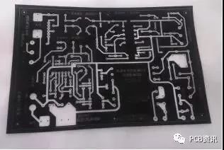
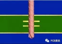
The legendary drill bit
For designers, the first consideration in lamination is symmetry. Since the board will be affected by pressure and temperature during the lamination process, residual stress remains in the board after lamination. If the laminated board is uneven on both sides, the stress on both sides will be different, causing the board to bend to one side, greatly affecting PCB performance. Additionally, even within the same plane, if the copper distribution is uneven, the resin flow speed at each point will differ; thus, areas with less copper will be thinner, while areas with more copper will be thicker. To avoid these issues, factors such as copper distribution uniformity, layer symmetry, and blind/buried hole design must be carefully considered during design. 5. Drilling Creates vias between the layers of the circuit board to achieve interlayer connectivity.
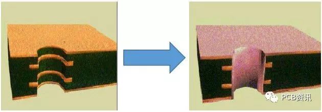
The legendary drill bit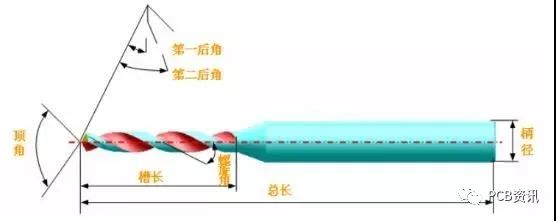 6. Copper Plating(1) Copper Deposition Also known as chemical copper, the PCB board after drilling undergoes a redox reaction in the copper plating tank, forming a copper layer to metallize the holes, allowing the originally insulated substrate surface to deposit copper, achieving electrical connectivity between layers.
(2) Board Plating Thickens the copper on the surface and inside the holes of the freshly deposited PCB to 5-8um to prevent oxidation and micro-etching of the thin copper before graphic electroplating.
7. Outer Dry Film The process is the same as that of the inner dry film.
8. Outer Graphic Electroplating, SES The copper layers on the holes and circuits are plated to a certain thickness (20-25um) to meet the final copper thickness requirements of the finished PCB. The unnecessary copper on the board surface is etched away, revealing the useful circuit graphics.
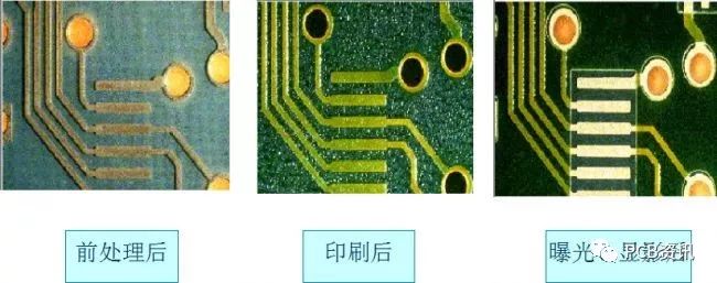
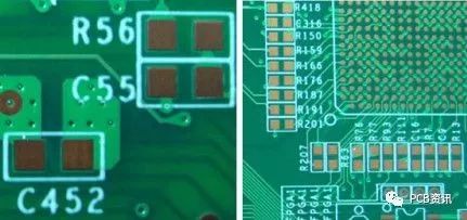
9. Solder Mask The solder mask, also known as anti-solder or green oil, is one of the most critical processes in PCB manufacturing, primarily applied through screen printing or coating solder mask ink, covering the board surface with a layer of solder mask. Through exposure and development, the pads and holes to be soldered are revealed, while other areas are covered with solder mask to prevent short circuits during soldering.
10. Silk Screen Characters Desired text, logos, or component symbols are printed on the board surface using screen printing, followed by exposure using ultraviolet light.
11. Surface Treatment Bare copper has good solderability, but long-term exposure to air can lead to moisture oxidation, tending to exist in the form of oxides, making it unlikely to maintain its original copper state for long. Therefore, surface treatment of the copper surface is necessary. The most basic purpose of surface treatment is to ensure good solderability or electrical performance.
Common surface treatments include: Tin spraying, gold immersion, OSP, tin immersion, silver immersion, nickel-palladium, electroless gold, and gold fingers.
12. Shaping The PCB is cut into the required external dimensions using a CNC shaping machine.
13. Electrical Testing Simulates the board’s state, powering it on to check electrical performance for any opens or shorts.
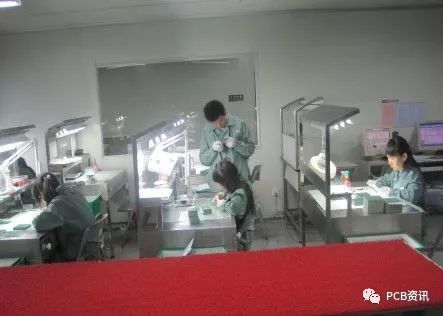
14. Final Inspection, Sampling, Packaging Inspects the board’s appearance, dimensions, hole diameter, board thickness, markings, etc., to meet customer requirements. Qualified products are packaged into bundles for easy storage and transport.
6. Copper Plating(1) Copper Deposition Also known as chemical copper, the PCB board after drilling undergoes a redox reaction in the copper plating tank, forming a copper layer to metallize the holes, allowing the originally insulated substrate surface to deposit copper, achieving electrical connectivity between layers.
(2) Board Plating Thickens the copper on the surface and inside the holes of the freshly deposited PCB to 5-8um to prevent oxidation and micro-etching of the thin copper before graphic electroplating.
7. Outer Dry Film The process is the same as that of the inner dry film.
8. Outer Graphic Electroplating, SES The copper layers on the holes and circuits are plated to a certain thickness (20-25um) to meet the final copper thickness requirements of the finished PCB. The unnecessary copper on the board surface is etched away, revealing the useful circuit graphics.
9. Solder Mask The solder mask, also known as anti-solder or green oil, is one of the most critical processes in PCB manufacturing, primarily applied through screen printing or coating solder mask ink, covering the board surface with a layer of solder mask. Through exposure and development, the pads and holes to be soldered are revealed, while other areas are covered with solder mask to prevent short circuits during soldering.
10. Silk Screen Characters Desired text, logos, or component symbols are printed on the board surface using screen printing, followed by exposure using ultraviolet light.
11. Surface Treatment Bare copper has good solderability, but long-term exposure to air can lead to moisture oxidation, tending to exist in the form of oxides, making it unlikely to maintain its original copper state for long. Therefore, surface treatment of the copper surface is necessary. The most basic purpose of surface treatment is to ensure good solderability or electrical performance.
Common surface treatments include: Tin spraying, gold immersion, OSP, tin immersion, silver immersion, nickel-palladium, electroless gold, and gold fingers.
12. Shaping The PCB is cut into the required external dimensions using a CNC shaping machine.
13. Electrical Testing Simulates the board’s state, powering it on to check electrical performance for any opens or shorts.
14. Final Inspection, Sampling, Packaging Inspects the board’s appearance, dimensions, hole diameter, board thickness, markings, etc., to meet customer requirements. Qualified products are packaged into bundles for easy storage and transport.
[1] Eight Experiences to Master Switch Power Supply PCB Layout
[2] Packaging Diagram: Mastering These 17 Types of Component PCB Packages Makes Designing Boards Much Easier!
[3] Eight-Layer PCB Design, Computer Motherboard Design Analysis
[4] So Beautiful! How Can PCB Routing Be So Beautiful?
[5] What is PCB Reflow? How to Solve It?
[6] Exclusive Skills and Techniques from PCB Experts