This question has been asked by many people, including some students in electronics. In fact, this is not new. Although FPGA is not a new thing, it has indeed been in contact with very few people in the past 30 years. Currently, there are only about a thousand FPGA engineers in China (as seen in the “China Integrated Circuit Industry Talent White Paper”).
Why has the market suddenly become so enthusiastic about FPGA in recent years?
Let me just mention a few points:
1. AI, the need for computing power;
2. 5G, the need for communication;
3. Cloud, the need for acceleration;
4. Chips, the need for verification;
It is also because of the above points that Field-Programmable Gate Arrays (FPGAs) stand out as amazing devices.
In simple terms, FPGA is a chip (you can think of it as an advanced chip).
Full English name: Field-Programmable Gate Array
Chinese explanation: 可编程逻辑门阵列
Unique advantages: Reprogrammable + Low power consumption
What is the essential difference between FPGA and other chips?
Before the advent of FPGA, all integrated circuits could be seen as a finished house, which cannot change the main structure of the house once it is built. At the same time, a lot of materials will be wasted during the construction process.
FPGA is like all the materials needed to build a house. You can freely combine them to build whatever kind of house you want. If you build it poorly, you can rebuild it. This is why it is called programmable.
What is the difference between FPGA and CPU, GPU, ASIC?
For example, ready-made toy models in a mall, such as toy cars and castles, are made by the manufacturer for you. You can only buy what you like. If you buy a toy car with four wheels and find that four wheels are not fun, but you actually want a tricycle, you can’t do anything about it; you can only spend more money to buy another one. This is equivalent to ASIC;
If you buy a game console, you need to insert a card to play different games. Without a game card, it is just scrap metal. This is equivalent to CPU or ARM.
FPGA is equivalent to LEGO blocks. What you buy is a pile of parts (IOB, SLICE, blockram, etc. in FPGA), and components like wheels and roofs are highly integrated (equivalent to DCM, DSP, etc. in FPGA); players can build various models according to the drawings.
Logic devices (digital chips) can be roughly divided into standard devices and custom chips. Generally speaking, the more customized a logic device is, the more advantages it has in terms of performance (speed), integration (number of gates), and design freedom. However, correspondingly, the development costs related to design and manufacturing (Non-Recurring Engineering, NRE costs) are also quite high, and the turnaround time (Turn Around Time, TAT) from ordering to delivery will be longer.
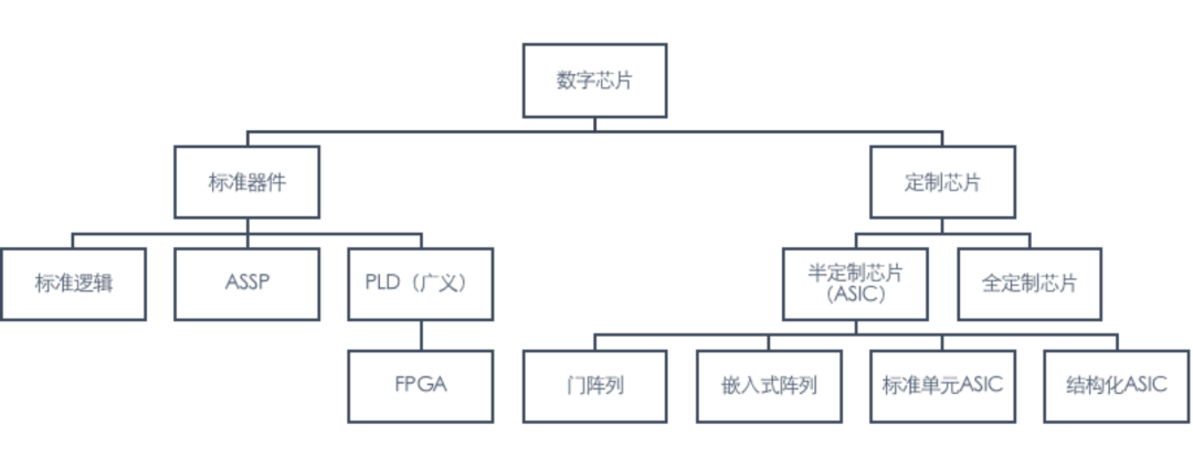
Custom chips can also be roughly divided into two types: fully customized chips designed from basic cells and semi-custom chips implemented using optimized standard cells. Semi-custom chips include standard cell ASICs (cell-based ASICs) designed using standard cell libraries; gate arrays formed by custom wiring on wafers where the standard cells have been pre-placed (all processes before wiring are completed); embedded arrays that lie between standard cell ASICs and gate arrays; and structured ASICs that minimize customization costs by providing general-purpose modules such as SRAM and clock PLL on gate arrays, etc. These processes are all aimed at reducing the NRE costs of custom chips and shortening TAT time.
On the other hand, there is a type of logic device in standard devices called Programmable Logic Devices (PLD), which differ from ASSP (Application-Specific Standard Products) that are fixed-purpose and cannot be customized. PLDs are a class of logic devices that can implement various logic circuits through programming. Due to the characteristics of allowing users to freely implement customized circuits through programming, PLDs have made great progress in recent years.
FPGA is a type of PLD that achieves the desired circuit by combining a large number of logic blocks within the device. FPGAs have a higher degree of design freedom than traditional (narrowly defined) PLDs and have a structure similar to gate arrays, which is why they are named FPGAs. FPGAs do not have any logic functions (unprogrammed state) when they are mass-produced. From the perspective of semiconductor manufacturers, they are a type of standard device that can be mass-produced. From the user’s perspective, they are a convenient ASIC that does not require high costs (NRE costs) for mold opening and can implement customized circuits at any time.
The FPGA/PLD industry has developed for decades, with more than 40 companies participating. Let’s review the history of the popularization, development, and changes of FPGA in chronological order.
1970s (FPLA and PAL emerge)
The early PLDs used a structure similar to PROM to implement programmable AND-OR arrays, which could use memory devices to remember circuit information. In 1975, Signetics released a programmable FPLA (Field Programmable Logic Array) based on fuse technology. Later, in 1978, MMI (now Lattice) simplified FPLA and developed a high-speed PAL (Programmable Array Logic) using bipolar transistor processes. Eventually, the PAL developed by MMI became widely adopted. The PAL used a fixed OR array with low delay and high-speed bipolar PROM, but it consumed a lot of power and could not be reprogrammed.
Early 1980s (GAL, EPLD, FPGA emerge) In the early 1980s, companies began to sell PLD products based on CMOS EPROM/EEPROM. These products had low power consumption and could be reprogrammed. During this period, Japanese semiconductor manufacturers, centered on DRAM technology, developed rapidly, while large American semiconductor companies performed relatively poorly. At this time, the main leaders in the PLD market were American start-ups. Various PLD architectures emerged, including Lattice’s GAL (Generic Array Logic, General Array Logic) established in 1983 and Altera’s EPLD (Erasable PLD, Erasable PLD) also established in 1983, with GAL being widely used. GAL was based on a fixed OR array structure compatible with PAL and used CMOS EEPROM as the programming memory element.
GAL and the aforementioned FPLA, PAL, and other single AND-OR array structures are collectively referred to as SPLD (Simple PLD), with integration levels ranging from several dozen to several hundred gates. As LSI integration levels continued to rise, the resource wastage problem of single AND-OR array structures became increasingly serious when manufacturing larger-scale PLDs than GAL. Therefore, FPGA and CPLD emerged as more flexible large-scale PLDs.
The first company to commercialize FPGA products was Xilinx, founded in 1984 by Ross H. Freeman and Bernard V. Vonderschmitt after leaving Zilog. Freeman produced the first practical FPGA chip (the XC2064 series) in 1985, which used a basic logic unit combining 4 inputs and 1 output LUT and FF. Shortly after, William S. Carter, who joined Xilinx, invented a more efficient interconnection method between units. These two inventions are known as the Freeman patent and the Carter patent, which are the most famous patents in PLD history. Ross H. Freeman was inducted into the US Inventors Hall of Fame in 2009 for inventing FPGA.
Xilinx’s FPGA products (named LCA) have the advantages of high design freedom, reprogrammability, and low power consumption (due to the use of CMOS SRAM). Inspired by Xilinx’s FPGA, Concurrent Logic produced FPGA products supporting partial reconfiguration, combining the results of MIT’s Petri network research. At the same time, the University of Edinburgh began research on virtual computers based on FPGA in 1985 and commercialized partially reconfigurable FPGA products through Algotronix (now Xilinx) in 1989. Among these products, the well-known ones are Atmel’s AT6000 and Xilinx’s XC6200, which are the ancestors of today’s dynamically reconfigurable FPGAs.
Late 1980s (Anti-fuse FPGA and CPLD emerge) In the mid to late 1980s, with the improvement of semiconductor integration and speed, anti-fuse FPGAs that could not be erased appeared. Companies that launched anti-fuse FPGA products include Actel (founded in 1985), QuickLogic (founded in 1988), and Crosspoint (founded in 1991).
However, at this time, the newly born FPGA did not have the performance expected by industry users, so many companies were still exploring large-scale PLDs based on other structures. Companies that had developed AND-OR array PLD products, such as Altera, AMD, and Lattice, were developing large-scale PLD products composed of multiple PLD blocks, which were later collectively referred to as CPLD (Complex PLD). Although CPLD did not match FPGA in terms of integration and design freedom, it had advantages such as fast speed, non-volatility, and easy erasure (using EPROM/EEPROM) compared to FPGA at that time. Therefore, until the early 1990s, they were both representative large-scale PLD products. However, in the late 1990s, the technology of SRAM-based FPGA rapidly developed in terms of both integration and speed, so the positioning of CPLD has now become a low-cost small-scale PLD product.
Entrepreneurship in the 1980s
The FPGA market has always been dominated by start-up companies in architecture research and productization. The first to commercialize FPGA products, Xilinx, was established in 1984 as a start-up. Altera and Lattice were also established at the same time and developed SPLD products, later joining the FPGA field. Actel was also a start-up that started slightly later than Xilinx. These four companies, after subsequent development, became the four major manufacturers in the FPGA market. Along with QuickLogic, which was founded later, these five companies that emerged in the 1980s gradually became the leaders in the FPGA market. Among large companies, only AT&T and Motorola developed proprietary FPGA architectures and productized them, but AT&T first entered the FPGA market through technology provided by Xilinx, and Motorola initially developed products after obtaining authorization from Pilkington, so they did not start from scratch. Additionally, Texas Instruments and Panasonic cooperated with Actel, while Infineon and ROHM Semiconductor cooperated with Zycad to participate in the FPGA market, but have now withdrawn.
Movements of Japanese Semiconductor Manufacturers and Large Semiconductor Manufacturers
Manufacturers of PLD founded in the 1980s, such as Lattice, Altera, Xilinx, and Actel, were all fabless companies without manufacturing facilities. They entrusted the chip manufacturing to Japanese semiconductor manufacturers that were rapidly growing in CMOS technology at that time. For example, Xilinx and Lattice entrusted production to Seiko Epson, while Altera entrusted production to Sharp. Actel not only entrusted manufacturing but also formed comprehensive alliances with Texas Instruments and Panasonic in manufacturing, technology, and sales. In the 1990s, there were also cases like FlashFPGA’s GateField cooperating widely with ROHM Semiconductor in manufacturing, technology, and sales. However, in recent years, the main force of PLD manufacturing has shifted to Taiwanese manufacturers such as UMC and TSMC, which have advanced CMOS technology.
At that time, large Japanese manufacturers focused only on DRAM in general products and gate arrays in customizable products, so they did not independently participate in the PLD market.
Large American semiconductor manufacturers such as Texas Instruments and National Semiconductor, which are good at manufacturing logic chips and memory products, have also participated in the development of bipolar AND-OR array PLD and CMOS EPROM/EEPROM PLD products. However, they have not been as proactive as specialized PLD manufacturers in developing new architectures and leading the market, and most have now withdrawn from the PLD market. Large enterprise AMD actively participated in the development of new architecture CPLD by acquiring MMI in 1987, but later to focus on the more promising CPU field, in 1996, it spun off the PLD business to its subsidiary Vantis, which was eventually sold to Lattice in 1999.
(1) Large-Scale Development of FPGA
In the 1990s, Xilinx and Altera respectively improved and expanded their XC400 and FLEX architectures, leading to rapid growth in the scale (number of gates) of logic circuits on FPGAs. In the early 1990s, the scale reached thousands to tens of thousands of gates, and in the late 1990s, it further developed to tens of thousands to hundreds of thousands of gates. Rapid prototyping environments using multiple FPGAs also emerged during this time. After entering the 1990s, FPGAs became rapidly popular, with more and more manufacturers such as AT&T (PLD business now belongs to Lattice), Motorola (now withdrawn from the PLD business), and Vantis (now Lattice) beginning to manufacture SRAM-based FPGAs. Japanese manufacturers such as Kawasaki Steel, NTT, and Toshiba also began to develop products but ultimately failed to bring them to market.
It is said that developing SRAM-based FPGAs might infringe on Xilinx’s basic patents (Freeman and Carter patents), so many manufacturers eventually abandoned productization. In 1993, Altera had a long legal dispute with Xilinx over patent issues regarding its SRAM-based PLD products (FLEX series, etc.). The two companies eventually reached a settlement in 2001, after which Altera also began to refer to its products as FPGAs.
In the late 1990s, some new types of FPGA products emerged. For example, GateField’s FPGA used Flash Memory as the programming element, which has advantages such as being erasable and non-volatile. DynaChip developed FPGA using high-speed ECL logic with BiCMOS technology.
Starting in the late 1990s, the integration and speed of FPGAs developed rapidly, especially in terms of integration, which distanced itself from CPLD. As a result, FPGA became the representative of large-scale PLD. On the other hand, the performance gap between FPGA and semi-custom products (especially gate arrays) gradually narrowed, successfully entering the market for semi-custom products (especially gate arrays).
Throughout the 1990s, the trend of systemization and large-scale development of FPGAs was very obvious, so the incorporation of hard core modules such as MPU and DSP also became inevitable. In 1995, Altera’s FLEX10K began to expand the application range of its products by incorporating memory blocks (memory blocks), and also incorporated PLL (Phase-Locked Loop) to enhance clock management and high-speed circuit design capabilities. From this period, FPGA truly became a mass-produced system widely used and rapidly popularized. In 1997, the logic scale reached 250,000 gates, and the main frequency reached 50~100 MHz. By 1999, the release of Xilinx’s new FPGA Virtex-E and Altera’s APEX20K promoted the further large-scale and high-speed development of FPGA, increasing the integration level to 1 million gates, marking the official arrival of the million-gate era of FPGA.
(2) Entrepreneurship in the 1990s
In the first half of the 1990s, start-up companies participating in the FPGA market included Crosspoint, DynaChip (Dyna Logic), and Zycad. Zycad originally mainly developed logic simulation EDA tools but later sold its EDA business and focused on the FPGA market, so it can also be regarded as a start-up in this period. However, at this time, the earlier Xilinx, Altera, Actel, and Quicklogic had already accumulated strong strength, making it difficult for Crosspoint and DynaChip to compete, leading to their exit from the market.
Crosspoint, founded in 1991, was the last company to produce anti-fuse FPGAs. The company applied for a patent in 1991, and its products were launched, but it ultimately ceased operations in 1996. Although it established a technology development and manufacturing sales contract with Japanese semiconductor giant Hitachi through its shareholder Japanese ASCII company less than a year after its establishment, and formed alliances with other large companies to plan participation in the FPGA market, this plan ultimately failed for various reasons. Crosspoint’s FPGA, in simple terms, is to place amorphous silicon anti-fuse through perforations in the metal wiring layer to achieve user-customizable gate arrays. Its feature is that it uses the finest granularity of transistors, allowing for transistor-level connections like gate arrays. If the transistor-level structure is consistent with CMOS logic gates, then theoretically, it will not produce the integration disadvantages of FPGA. This is the innovative technology of Crosspoint; similar FPGAs had never existed before, nor has there been any programmable devices that can achieve the same architecture as CMOS gate arrays afterward.
On the other hand, in the late 1990s, the two giants Xilinx and Altera performed strongly in the market, and new FPGA chip manufacturers did not emerge for some time. Many companies that started with FPGA cores or dynamically reconfigurable processors, especially the latter, emerged. However, most of these companies either got acquired or went bankrupt, and even those still operating have hardly achieved commercial success.
(1) The Million-Gate Era and System LSI
Entering the 2000s, FPGA began to show a trend of system LSI. As a processor IP developed and supported by FPGA manufacturers, Altera publicly released the Nios soft core processor. In the same year, Altera also launched the world’s first FPGA product with a hard core processor, Excalibur. Excalibur integrated an ARM processor (ARM922 and peripheral functions) and FPGA circuits on a single chip. In addition, Xilinx also launched the soft core processor MicroBlaze and produced FPGA products with PowerPC processor hard cores (Virtex II Pro).
In the process of system LSI, high-speed external interfaces are also important. At this time, FPGAs began to apply SERDES (Serializer-Deserializer) circuits and LVDS (Low Voltage Differential Signaling) to achieve high-speed serial communication interfaces. At the same time, to meet the performance needs of image processing and other operations, high-performance modules such as digital signal processor blocks (DSP blocks) and multi-input logic blocks with high area efficiency ratio were added in addition to general logic blocks, significantly improving integration and circuit performance. Then, to meet different users’ needs for hard core IP, manufacturers also developed various sub-series products for different field users to choose from.
Taking Altera as an example, the company launched high-end FPGA products that integrated these innovative evolutions, such as Stratix (2002, 130nm). The subsequent products Stratix II (2004, 90nm), Stratix III (2006, 65nm), and Stratix IV (2008, 40nm) upgraded every two years. In 1995, when FLEX10K was released, its logic circuit scale was about 100,000 gates, and the maximum internal clock was 100 MHz. By 2009, its logic circuit scale had reached 15 million gates (8.4 million logic and DSP blocks), increasing 150 times in 15 years, and the maximum internal clock frequency also reached 600 MHz. On the other hand, Xilinx’s high-end FPGA products Virtex II Pro (2002, 130 nm), Virtex-4 (2004, 90nm), Virtex-5 (2006, 65nm), and Virtex-6 (2009, 40nm) also upgraded approximately every two years.
Since the logic chip process is updated approximately every two years, the evolution of FPGA after 2000 has basically kept pace with process upgrades.
(2) Emerging Manufacturers in the 2000s
The two most basic patents related to FPGA, the Carter and Freeman patents, were the biggest obstacles for emerging manufacturers considering entering the FPGA chip market. However, as time passed, the Carter patent expired in 2004 and the Freeman patent expired in 2006. Taking this opportunity, many new FPGA companies emerged during this period, such as SiliconBlue Technologies, Achronix Semiconductor, Tabula, Abound Logic (formerly M2000), and Tier Logic, etc.
SiliconBlue developed an ultra-low power FPGA series product, iCE65, aimed at portable devices based on TSMC’s low-leakage 65nm process, which has only 1/7 of the working power consumption and 1/1000 of the standby power consumption compared to traditional SRAM-based FPGAs.
Achronix developed the Speedster series based on high-speed FPGA research from Cornell University, characterized by using asynchronous circuits to transmit data tokens. Data tokens combine past FPGA data and clock for handshake data transmission. The company’s initial product, SPD60 (TSMC 65nm), has a throughput three times that of previous FPGAs, around 1.5GHz.
Tabula’s technical feature is to utilize the advantages of dynamic reconfiguration to implement multiple functions on the same logic unit, thereby reducing FPGA costs. Compared to other ASIC products, the price of large manufacturers’ FPGAs is relatively high, and Tabula adopted a pricing strategy to attack this point, which is typical of start-up companies. The company’s ABAX series FPGA uses a unique dynamic reconfiguration technology to dynamically switch logic units, allowing for large-scale circuits to be implemented with fewer resources. Specifically, it generates high-speed clocks inside the FPGA by multiplying external input clock signals and uses high-speed clock signals to drive logic circuits and circuit reconfiguration mechanisms. Therefore, even if the physical logic circuit scale is fixed, it can achieve time-sharing multiplexing of logic circuits through high-speed switching, thus obtaining a larger effective logic scale. Tabula refers to this structure that adds a time dimension to increase effective logic scale on a two-dimensional chip as 3D FPGA.
Abound Logic has released large-scale FPGA products characterized by Crossbar Switch and scalable architecture, but ceased related business in 2010. Tier Logic developed unique monolithic 3D-FPGA technology by implementing configuration SRAM above CMOS circuits using amorphous silicon TFT, but also ceased operations in 2010 due to funding shortages.
(1) Development of Processes and New Technology Trends
In 2010, both Xilinx and Altera launched 28nm FPGAs and began supplying them in the spring of 2011, further consolidating FPGA’s advantage over ASIC. These two largest FPGA manufacturers, in addition to their previous high and low-end FPGAs, also added mid-range product lines. For example, Xilinx changed its foundry partner from UMC to TSMC, and the entire product line of Xilinx 7 series (high-end FPGA Virtex-7, mid-range FPGA Kintex-7, low-end FPGA Artix-7) adopted 28nm manufacturing process, improving performance while reducing power consumption. Now, the latest FPGAs from both Xilinx and Altera are produced by TSMC.
Next, let’s explain the new trends of 28nm FPGA technology.
(a) The Trend of SoC in the New Era
Although both Xilinx and Altera launched the first generation of SoC FPGAs with hard core processors around 2000, these products were relatively short-lived. Later, FPGAs with soft core processors became widely used. However, with the advancement of processes, FPGA with hard core processors gradually began to meet market demand in terms of performance and cost. In addition, this period coincided with the gradual elimination of 32-bit processors from the market. Driven by these internal and external factors, SoC FPGAs that integrate CPU cores and peripheral processing circuits aimed at embedded processors such as ARM finally emerged. These products are referred to as SoC FPGA, programmable SoC, or SoPD (System on Programmable Device), etc. For example, Xilinx launched the Zynq brand with the Zynq-7000 series products. This series of products integrates Xilinx’s 28nm 7 series programmable logic on the basis of the ARM Cortex-A9 MPCore processor. Altera’s Cyclone V series SoC FPGA products also integrated dual-core ARM Cortex-A9 MPCore processors and FPGA on the same chip.
(b) Partial Reconfiguration
Partial reconfiguration refers to the function of reconfiguring specific parts of an FPGA while allowing the remaining parts to continue working without interruption. Xilinx’s high-end FPGA devices after Virtex-4 and their development tools (ISE version 12 and above) support partial reconfiguration. Altera also began to support partial reconfiguration from Stratix V onwards. The fact that both major FPGA manufacturers officially support partial reconfiguration technology indicates a strong market expectation for this technology.
Xilinx manufactured the first 2.5D-FPGA product by stacking and connecting multiple FPGA chips arranged in a two-column basic plane on a silicon interposer. Although the ideal 3D chip is to vertically stack multiple chips with TSV (Through Silicon Via), some chips are difficult to make TSV, and chips containing a large number of TSVs have low yield, leading to high manufacturing costs. The highly anticipated 2.5D technology only requires stacking two layers of chips without using TSV, thus alleviating these problems and achieving near 3D performance. The Virtex-7 2000T, manufactured based on TSMC’s 28nm HPL process, is the largest FPGA in the industry, integrating 6.8 billion transistors, with its 2 million logic units equivalent to 20 million ASIC gates.
Xilinx developed the XA Artix-7 FPGA, which complies with the AEC-Q100 standard for automotive applications, based on the Artix-7 FPGA, as well as programmable SoC forms of XA Zynq-7000 products. Xilinx’s design tools have also passed the ISO-26262 certification for functional safety standards implemented by third parties. In addition, Altera and Lattice are also working on their respective automotive solutions.
(e) C Language Development Environment
Recently, FPGA manufacturers have begun to provide development environments for FPGA design using C language. Xilinx’s high-level synthesis tool Vivado HLS supports users to directly synthesize FPGA hardware from C, C++, or System C code without the need to write RTL. This tool is also compatible with ISE and Vivado design environments. On the other hand, Altera actively promotes the application of OpenCL. OpenCL is developed based on the C language and can deploy code to various platforms such as CPU, GPU, DSP, and FPGA. Altera aims to popularize its FPGA products in parallel computing hardware accelerator applications by providing support for OpenCL.
There are also some new technologies. For example, optical FPGAs equipped with high-bandwidth optical communication interfaces to meet the growing demand for communication bandwidth, or radiation-hardened FPGAs that can withstand strong radiation.
FPGA Processes and Roadmap
After the 28nm process, Xilinx launched the UltraScale series based on the 20nm process. This series includes two sub-series, Kintex UltraScale and Virtex UltraScale, with Virtex UltraScale being the largest, equivalent to 50 million ASIC gates. The UltraScale series is mainly manufactured by TSMC’s 20nm process, with only the high-end model of Virtex UltraScale using TSMC’s 16nm FinFET process. On the other hand, Altera’s next-generation Generation 10 FPGA, including Arria 10 FPGA and Stratix 10 FPGA, are SoC products equipped with embedded hard core processors. Generation 10 devices are manufactured using the industry’s most advanced Intel 15nm FinFET process and TSMC’s 20nm process, with the high-end Stratix 10 products achieving frequencies of over 1GHz.
Logic chips have always followed the pace of process technology development, updating every two years. Compared to the development of Intel processors, FPGA after 2000 also basically conforms to this development rhythm. ASICs still closely follow advanced processes until the early 21st century, but in the last decade, except for some applications like game consoles, most products still use 130~90nm processes, essentially staying at the level of a decade ago.
FPGAs, like general-purpose processors, continuously use the most advanced process technology to launch new products. In the future, with the advancement of 28nm, 20nm, and 16/14nm processes, the processes used by FPGAs will be three to four generations ahead of ASICs, and their performance will be sufficient to compete with ASIC products at 130nm, 90nm, and even 65nm.
Monopolization and Industry Restructuring
Entering the 2010s, the monopolization of the FPGA industry has intensified. The two largest companies in the industry, Xilinx and Altera, occupy more than 80% of the market share, while most of the remaining 20% is shared by core manufacturers Lattice and Actel. Actel, the fourth largest, was acquired by Microsemi, which focuses on high-reliability semiconductors, in October 2010. Products launched under the Microsemi FPGA brand are mainly based on Flash and anti-fuse non-volatile FPGAs.
Among the FPGA manufacturers that started in the 1980s, QuickLogic also once sold anti-fuse FPGAs, but later this company changed its product strategy and left the FPGA market, focusing on custom area programmable CSSP (Customer Specific Standard Products). Compared to the overall programmable structure of FPGA chips, CSSP only provides a part of the programmable area, while the remaining part uses standard circuits with a unified interface, allowing customers to customize specific parts of the product. Atmel’s FPGA technology was mainly used in combination with its own AVR microcontrollers, and the company exited the mainstream FPGA market like QuickLogic.
Emerging FPGA manufacturers that started in the mid-2000s, such as SiliconBlue, which focused on ultra-low power FPGAs, were acquired by Lattice at the end of 2011. Lattice later launched the iCE40 series products based on 40nm. Additionally, Tabula, which focused on low-cost FPGAs using dynamic reconfiguration technology, went bankrupt in March 2015. Achronix also launched the Speedster22i FPGA series based on Intel’s 22nm process in 2015.
In recent years, the semiconductor industry as a whole has entered a major restructuring era, with several significant mergers and acquisitions occurring. At the same time, the FPGA industry has also changed. The most representative case is Intel’s acquisition of FPGA giant Altera in June 2015. The final acquisition amount was $16.7 billion, nearly ten times Altera’s revenue at that time, making it the largest acquisition in Intel’s history. Intel recognized that to continue to dominate the growing data center and IoT processor markets, FPGA technology would become an indispensable technology.
Following this event, Qualcomm and Xilinx announced a strategic partnership in November 2015. The two companies will integrate their respective strengths—ARM processors for high-end servers and FPGA technology—to provide solutions for the data center market. The results of this collaboration will cover cloud computing infrastructure areas such as big data analysis, machine learning, and storage.
In November 2015, Xilinx announced the news of its long-standing strategic alliance with IBM. By using Xilinx’s FPGA in IBM’s Power Systems to develop accelerators for specific applications, it can achieve energy-efficient data center systems, thereby improving the performance of applications such as machine learning, virtualization networks, high-performance computing, and big data analysis.
This series of strategic partnerships is seen as a response to Microsoft’s (Microsoft) lead in developing the Catapult acceleration system in collaboration with Altera.
Basic Knowledge Required to Understand FPGA
FPGA (Field Programmable Gate Array) is a semiconductor device that can implement the desired logic circuits required by users through reprogramming. To facilitate understanding of FPGA design and structure, we will first briefly introduce some basic knowledge of logic circuits.
Logic AlgebraIn logic algebra, all variable values can only be 0 or 1. Logic algebra is an algebraic system formed by three operations related to logical values (0 and 1): logical AND (AND), logical OR (OR), and logical NOT (NOT), also called Boolean algebra.
As shown: the binary operations defining logical AND and logical OR, as well as the unary operation defining logical NOT, are listed. Here, the three operations are represented using the operators “.”, “+”, and “¬”. Logical AND xy means the operation where the result is 1 when both x and y are 1. Logical OR x+y means the operation where the result is 1 when at least one of x or y is 1. Logical NOT “x” is a unary operation that takes the opposite logical value: if x is 0, the result is 1; conversely, if x is 1, the result is 0.
Logic algebra satisfies the theorems shown in Table 1-2. Here, the symbol “=” indicates that the calculation results on both sides are always equal, that is, equivalent. If the logical values in a logical expression are exchanged with logical operations “AND” and “OR”, and the new logical expression obtained after the exchange remains unchanged in operation order, then the new logical expression is called the dual of the original logical expression. In logic algebra, if the logical expression of a theorem holds, its dual also holds.
|
Logical AND (·)
|
Logical OR (+)
|
Logical NOT (¬)
|
|
0·0=0 0·1=0 1·0=0 1·1=1
|
0+0=0 0+1=1 1+0=1 1+1=1
|
0=1 1=0
|
1-1
Logic algebra satisfies the theorems shown in Table 1-2. Here, the symbol “=” indicates that the calculation results on both sides are always equal, that is, equivalent. If the logical values 0 and 1, and the logical operations “AND” and “OR” in a logical expression are exchanged, and the new logical expression obtained after the exchange remains unchanged in the operation order, then the new logical expression is called the dual of the original logical expression. In logic algebra, if the logical expression of a theorem holds, its dual also holds.
|
Zero Element x·0=0, x+1=1
|
Unit Element x·1=x, x+0=x
|
|
Idempotent Law x·x=x, x+x=x
|
Complementary Law x·x=0, x+x=1
|
|
Double Negation x=x
|
Commutative Law x·y=y·x, x+y=y+x
|
|
Associative Law (x·y)·z=x·(y·z), (x+y)+z=x+(y+z)
|
|
Distributive Law x·(y+z)=(x·y)+(x·z), x+(y·z)=(x+y)·(x+z)
|
|
Absorption Law x+(x·y)=x, x·(x+y)=x
|
|
De Morgan’s Laws x+y=x·y, x·y=x+y
|
Logical Expressions
A logical expression is a formula used to describe an operation process, composed of logical operators, any number of logical variables, and necessary parentheses and constant values 0 or 1. For a logical expression containing n logical variables x1, x2, x3, …, xn, we first substitute the logical values 0 or 1 into each logical variable, forming arbitrary combinations (a total of 2^n combinations), and then calculate these combinations according to the calculation steps of the logical expression to get a result of 0 or 1. In other words, a logical expression defines a logic function F(x1, x2, x3, …, xn) with a certain logical function.
Any logical function can be described by a logical expression, and there can be multiple logical expressions that describe the same logical function. The standard form of a logical expression refers to a situation where, by adding restrictions on the form of the expression, a logical function corresponds to only one logical expression. In a logical expression, the logical variables appear in the form of original variables or inverted variables. Original variables and inverted variables are collectively referred to as literals. The logical AND of literals (each literal cannot appear multiple times) is called a product term, and the logical OR of product terms is called a sum of products. A product term that contains all literals is called a minterm, and a sum of products composed of minterms is called a standard sum of products (standard product).
Interchanging the logical AND of standard products and logical OR is the standard product of sums. The logical OR of literals (each literal cannot appear multiple times) is called a sum term, and the logical AND of sum terms is called a product of sums. A sum term that contains all logical variables is called a maxterm, and a product of sums composed of maxterms is called a standard product of sums (standard sum).
Truth Tables
In addition to logical expressions, there are other methods to describe logical functions, such as truth tables and logic gates. By listing the output values for all possible input combinations of a logical function, we can obtain a truth table.For combinational logic circuits, as long as all possible inputs and their corresponding output values are listed, the circuit function can be completely described. Therefore, the circuit function is usually described using truth tables.The number of inputs is n, and the number of combinations in the truth table is 2^n.In the truth table, it is necessary to record the output value corresponding to each set of input values.
The logical expression that implements the function defined by the truth table can have many forms, while the truth table describing the logical function is unique. Although a logical expression describes only one logical function, a logical function can be described by countless equivalent logical expressions.The circuit that implements the function defined by the truth table is called a Look-up Table (LUT), which is the basic unit of mainstream FPGAs today.
There are two ways to derive the logical expression from the truth table: the “sum of products expression” and the “product of sums expression”. In the rows of the truth table where the output is 1, take the product terms (minterms) of the input variables and OR these minterms to obtain the standard sum of products expression; conversely, in the rows of the truth table where the output is 0, take the inverted variables of the input variables (maxterms) and AND these maxterms to derive the standard product of sums expression.The example in Figure 1-1 demonstrates how to derive a logical expression from a truth table.
Excerpt from “Principles and Structures of FPGA”.


