Source: Semika
Original Author: Semika
Testing is an important means to ensure functionality and yield.Chip testing can be mainly divided into two parts.CP (chip probing) and FT (final test).Some chips will also undergo SLT (system level test).Additionally, some specific requirement chips need reliability testing.
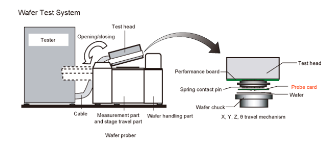
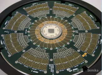
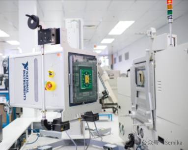
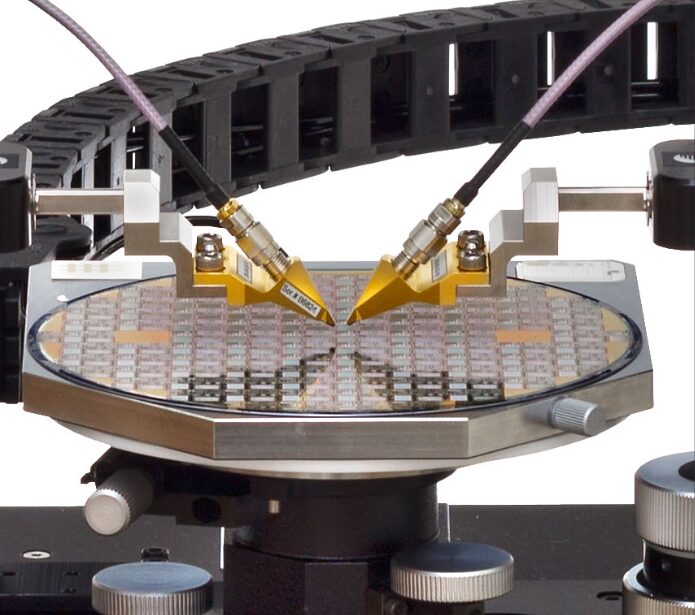
CP (Chip Probing) testing, also known as wafer testing, is the testing of the wafer before the chip is packaged. This allows for the elimination of problematic chips before packaging, saving costs on packaging and FT. CP testing is positioned between wafer manufacturing and packaging in the entire chip manufacturing process. After wafer (Wafer) production is completed, thousands of bare DIE (unpackaged chips) are evenly distributed across the entire wafer. Since the chips have not yet been diced and packaged, all pins are exposed, and these extremely small pins need to connect to the tester through finer probes (Prober).The following image illustrates the CP automated testing system.
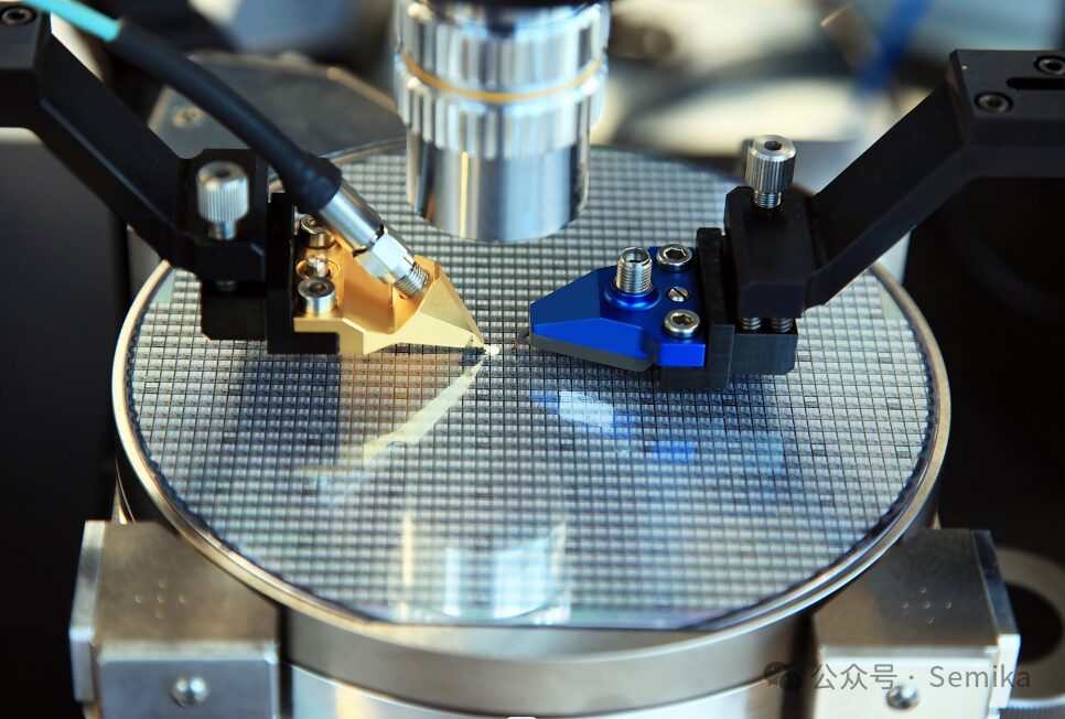
CP can be visualized as testing the wafer with probes, as shown in the image below:
However, in practice, the number of probes is very large, with thousands to tens of thousands of probes used on the probing station. The probing station is used to support the wafer platform, allowing every die and bond pads in the wafer to connect to the probes on the Probe card. It can also precisely shift, allowing for a different die to connect to the Probe card’s probes after each test, ensuring that every die on the wafer is tested.
CP testing mainly measures the following aspects:
-
Scan. Scan is used to check whether the chip’s logic functions correctly;
-
Boundary SCAN. Boundary SCAN is used to check whether the chip’s pins function correctly;
-
Memory. Chips often integrate various types of memory (e.g., ROM/RAM/Flash). To test the memory’s read/write and storage functions, BIST (Built-In Self Test) logic is usually added during design for self-testing. The chip enters various BIST functions through special pin configurations, and after self-testing, the BIST module feeds back the test results to the Tester;
-
DC/AC Test. DC testing includes Open/Short tests of chip Signal PINs, PowerShort tests of power PINs, and checks to see if the chip’s DC current and voltage parameters meet design specifications;
-
RF Test. For wireless communication chips, RF functionality and performance are crucial. RF testing in CP checks the RF module’s logic functions, while FT must further test RF performance;
-
Other Function Tests. Other functional tests of the chip check whether other important functions and performance meet design specifications.
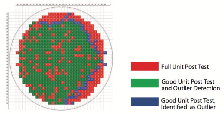
The closer a die (a small square, i.e., an unpackaged chip) is to the edge of a wafer, the higher the probability of it having issues.
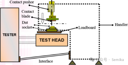
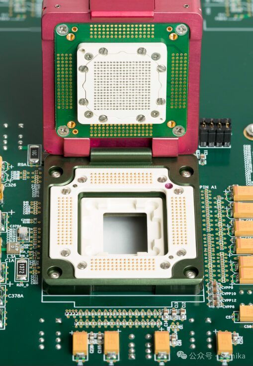
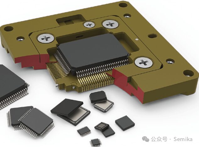
FT (final test) is the ultimate testing conducted after the chip is packaged. FT testing is a chip-level test that establishes electrical connections between the automated test equipment (ATE) and the packaged chip through a test board (Loadboard) and test socket (Socket). The purpose of FT testing is to filter out products that meet design specifications.
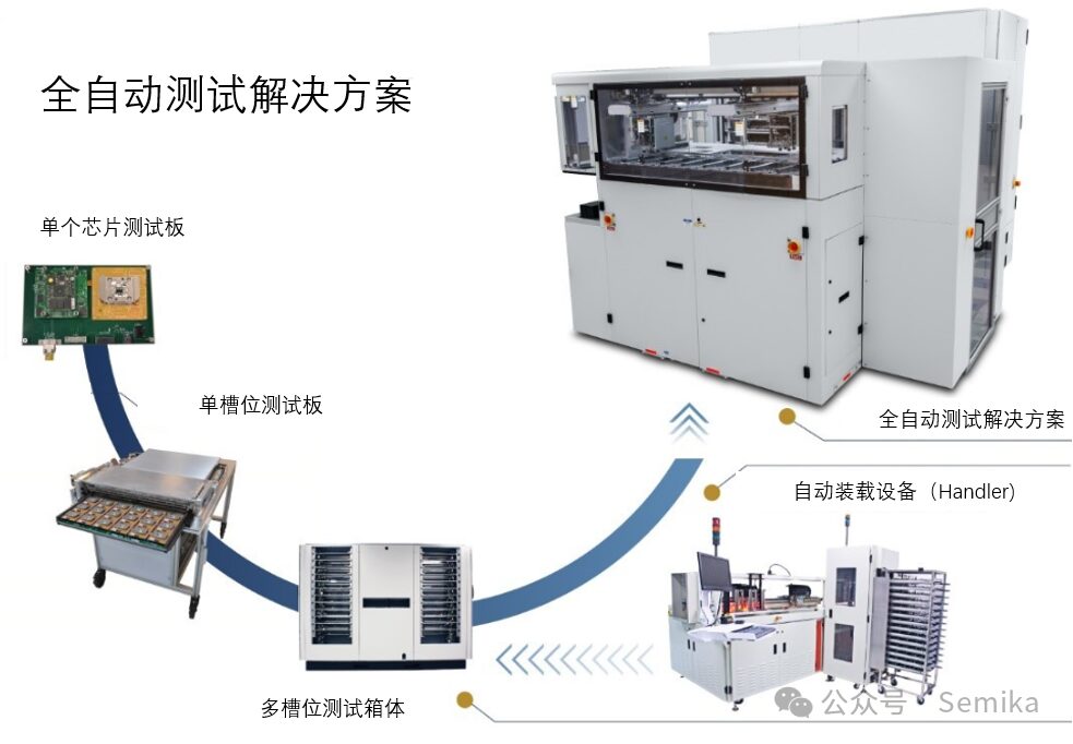
The structure of the FT testing system is shown in the image below:
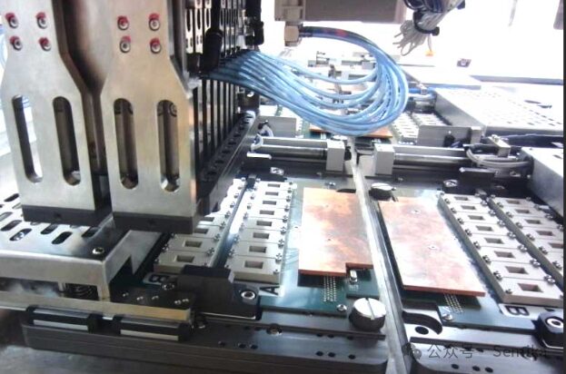
Required hardware for FT testing includes the test board, test socket, ATE (Automated Test Equipment), and Handler. The Handler, also known as the automated sorting machine, is used to automate FT testing.
Only when the handler is combined with the tester and connected to the interface can testing occur. The action involves the handler’s arm placing the chip into the socket, and then the contact pusher presses down. This ensures that the chip’s pins correctly contact the socket, sending a start signal through the interface to the tester. After testing is complete, the tester sends back the binning and EOT (end of test) signal. The handler then performs sorting actions.
FT testing items are also determined based on the chip’s functions and characteristics. Common FT test items usually include:
-
Open/short test, which checks whether the chip pins have open or short circuits;
-
DC test, which checks the device’s DC current and voltage parameters;
-
Eflash test, which checks the embedded flash functionality and performance, including read/write parameters, power consumption, and speed;
-
Function test, which tests the chip’s logical functions;
-
AC test, which verifies AC specifications, including the quality of AC output signals and their actual parameters;
-
RF test, which validates the functionality and performance parameters of chips with RF modules;
-
Additionally, there is DFT test, which includes scan design and built-in self-test (BIST).
SLT stands for System Level Test. SLT is used when other testing coverage cannot be met. It is also used to control costs since ATE testing is relatively expensive. SLT testing places chips on a test board, which can be used to verify various chip functions. By controlling multiple testing machines, batch testing can be achieved.
SLT testing requires hardware including test boards, test sockets, Handler, Change Kit, and test host with connecting cables. SLT testing is a customized test, and the software part is flexible, not requiring development on an automated testing platform, allowing testing engineers to develop it independently. SLT testing typically includes chip function testing, high-speed interface testing, and DDR memory-related testing. Similar to FT testing, the program will physically bin the chips based on test results, whether Pass or Fail.
In addition to these three main tests, some chips may also undergo reliability testing, which includes:
-
ESD, which is electrostatic discharge immunity testing;
-
-
HTOL, which is high-temperature operating life testing;
-
LTOL, which is low-temperature operating life testing;
-
TCT, which is temperature cycling testing;
-
HAST, which is high-accelerated stress testing for temperature and humidity;
-
Other special requirement tests;
Chip testing is highly complex and is a mass production task, so large-scale automated testing is the only solution; manual or bench testing cannot accomplish such tasks.
In semiconductor testing, the tester, sorter, and probing station are three key pieces of equipment that work together to ensure testing accuracy and efficiency.
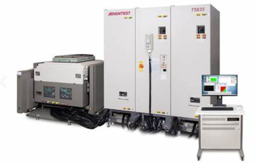
The tester is one of the core devices in semiconductor testing. It tests the chip’s electrical characteristics and functional verification by providing power, instruments, and signal processing. Testers typically have multiple slots for inserting chips to be tested. Depending on different testing needs, testers can perform various tests including voltage, current, power, frequency, and timing. They can automatically execute test programs and generate test reports and data analysis results.
Key technologies for testers include test program development, test point wiring, signal acquisition, and processing. To improve testing efficiency and accuracy, testers often incorporate advanced technologies such as high-speed digital signal processors, analog converters, and clock management. Additionally, testers need to have good flexibility and scalability to adapt to changes in chip types and testing requirements.
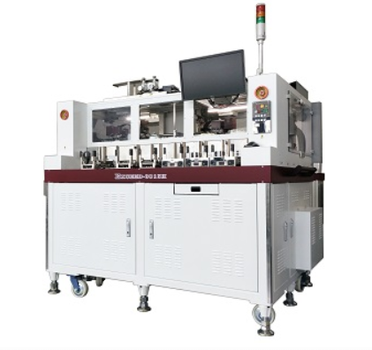
The sorter is another important device in semiconductor testing. It is primarily used to classify and sort tested chips according to specific standards or requirements. Sorters typically utilize high-speed image processing and recognition technologies to perform optical inspection and differentiation of chips, determining their quality and compliance.
Key technologies for sorters include image sensors, image processing algorithms, and motion control systems. Through optical inspection and image processing, sorters can quickly and accurately identify and classify chips, removing defective products, ensuring that only high-quality chips proceed to the next production stage. The efficiency and accuracy of sorters are crucial for improving production efficiency and reducing defect rates.
The probing station is one of the key devices used in chip testing. It provides a platform for fixing and supporting the test probes, ensuring stable contact between the probes and the test points on the chip. The main functions of the probing station include providing a stable mechanical structure, reliable probe fixation and adjustment, good conductivity, and insulation properties.
Key technologies for probing stations include mechanical structure design, probe fixation and adjustment mechanisms, and conductive material selection and processing. By precisely controlling the position and pressure of the probes, probing stations ensure good contact between the probes and the chip, providing a stable testing environment. The high precision and stability of probing stations are critical for the accuracy and reliability of test results.
END
Reprinted content only represents the author’s views
Does not represent the position of the Semiconductor Institute of the Chinese Academy of Sciences
Editor: March
Responsible Editor: Six Dollar Fish
Submission Email: [email protected]
1. The Semiconductor Institute has made progress in the research of bionic coverage-type neuron models and learning methods
2. The Semiconductor Institute has made significant progress in inverted structure perovskite solar cells
3. Why is copper used as interconnect metal in chips?
4. What exactly is 7nm in chips?
5. Silicon-based integrated optical quantum chip technology
6. How unusual is the quantum anomalous Hall effect? It may bring the next information technology revolution!