
–[Paper Update – Issue 225]-
Nano Letters – Monolithically Integrated Metasurface on a PCSEL for Depth Perception – National Yang Ming Chiao Tung University
Click the blue text to follow us
Column Introduction
「“The Paper Update” column aims to succinctly share research findings published in high-level journals within the Metasurface field over the past week, helping readers stay informed about the latest developments in the field. If you have any suggestions regarding the writing style or content of the column, please feel free to leave a message. We will gradually open other columns in the future, so stay tuned.」
1
Basic Information of the Paper
Title:
Monolithically Integrated Metasurface on a PCSEL for Depth Perception
Authors:
Wen-Cheng Hsu (National Yang Ming Chiao Tung University, College of Optoelectronics);
Wen-Chien Miao (National Yang Ming Chiao Tung University, College of Optoelectronics);
Corresponding Author Yu-Heng Hong (Foxconn Research Institute, Semiconductor Research Center);
Corresponding Author Hao-Chung Kuo (National Yang Ming Chiao Tung University, College of Optoelectronics);
Corresponding Author Yao-Wei Huang (National Yang Ming Chiao Tung University, College of Optoelectronics)
Publication Date:
July 11, 2025 (submitted on May 9, 2025, revised on June 29, 2025, accepted on June 30, 2025)
Published Journal:
Nano Letters (JCR-Q1, IF=9.1)

2
Key Figures and Images from the Paper
Abstract:
Dot projectors are core components for depth perception in modern consumer electronics (such as smartphones and augmented reality devices), widely used in computational imaging, machine vision, and privacy protection technologies. However, existing designs are limited by their large size and high power consumption. This study achieves the first monolithic integration of a metasurface hologram with a photonic crystal surface-emitting laser (PCSEL), constructing a chip-level structured light projector that significantly reduces device size and power consumption while maintaining practical 3D sensing capabilities. The wafer-level design has a compact volume of only 0.025 mm³, approximately 2450 times smaller than commercial DOE-VCSEL dot projectors, with a power consumption reduction of 28.7%. This integration strategy offers excellent manufacturing compatibility, bringing transformative advancements to compact transceiver systems and is expected to drive the development of next-generation biometric, augmented reality, and consumer electronics applications.
Important Images:
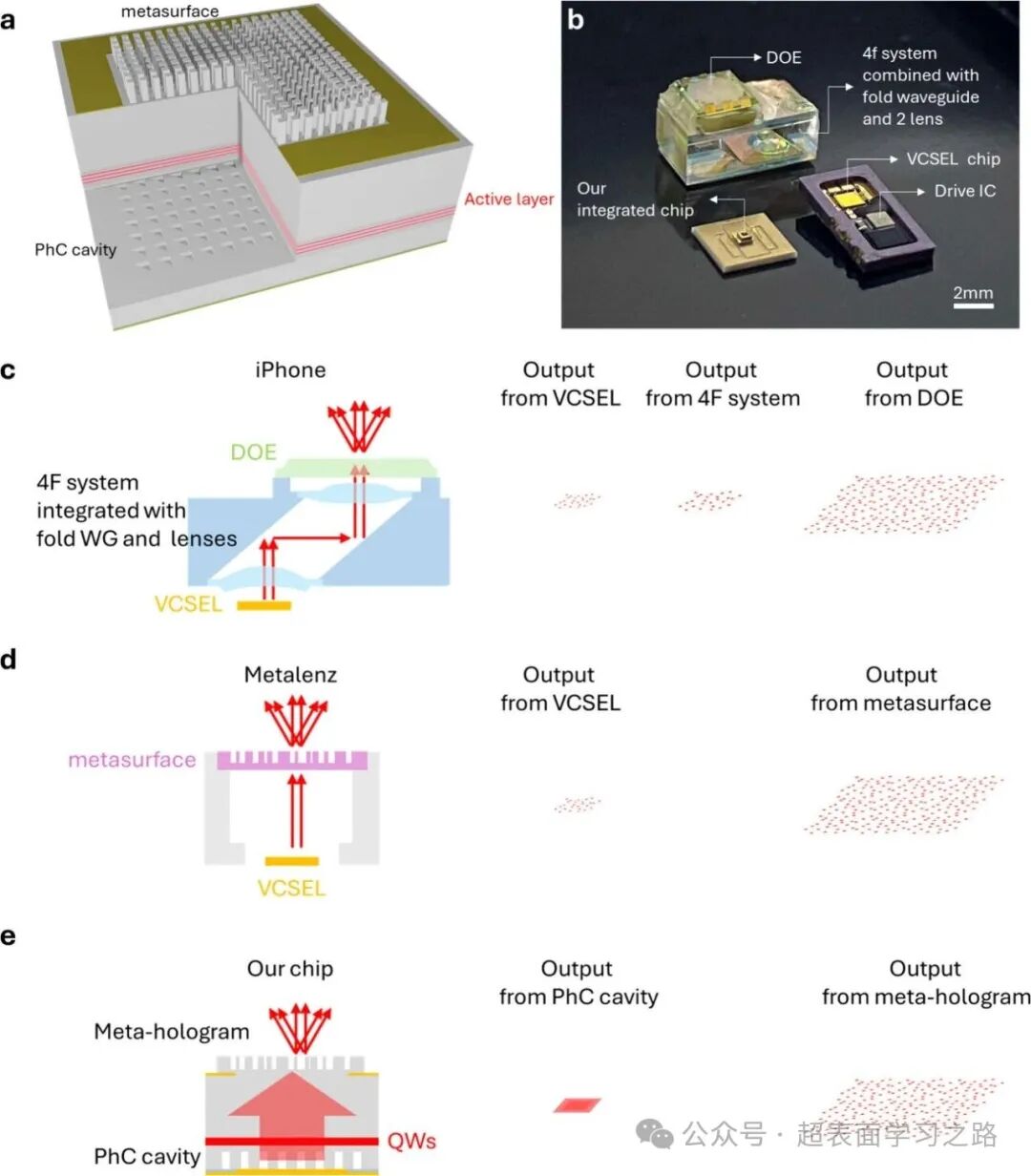
Figure 1. Design of the Structured Light Projector
a 3D schematic of the monolithically integrated chip-level structured light projector: the metasurface is fabricated in situ on the PCSEL (photonic crystal surface-emitting laser).
b Size comparison: the integrated chip from this study (mounted on a carrier and packaged as an SMD device) versus the discrete component volume of a commercial dot projector (Face ID of iPhone X).
c Schematic diagram of the commercial iPhone dot projector architecture.
d Schematic diagram of the Orion dot projector (ML1DP18MS, Metalenz).
e The proposed dot projector architecture in this study: metasurface integrated with PCSEL, significantly simplifying the structure.
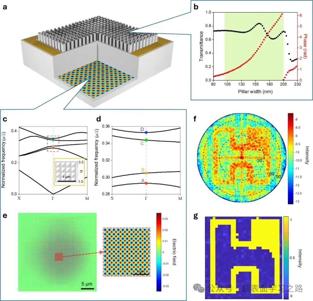
Figure 2. Hybrid Simulation and Results of the Monolithically Integrated Structured Light Projector
a 3D schematic of the hybrid simulation setup: GaAs metasurface hologram placed on the substrate, with a photonic crystal (PhC) mode as the light source below.
b Design principle of the metasurface hologram: based on the GS algorithm and super-atom library, using a propagation phase design strategy.
c Band structure of GaAs PhC with triangular air holes (calculated using Lumerical finite-difference eigenmode solver), with an inset showing a 2D schematic of the PhC structure.
d Enlarged view of the band structure near the Γ2 point in (c).
e Electric field distribution of the finite-size PhC mode (Lumerical FDTD simulation).
f Far-field projection of the “Foxconn” logo obtained from the hybrid simulation.
g Numerical projection of the “Foxconn” logo calculated using the GS algorithm.
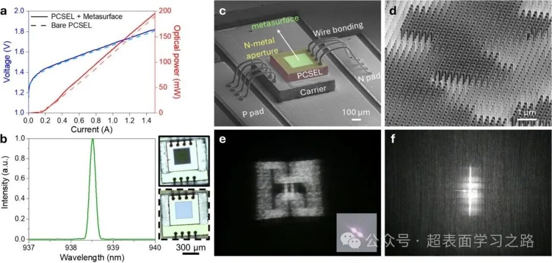
Figure 3. Device Characteristics, SEM Images, and Optical Performance
a Output light power-current-voltage (L−I−V) curves of the PCSEL with metasurface (solid line) versus bare PCSEL (dashed line).
b Emission spectrum of the metasurface-integrated PCSEL, with an inset showing optical microscope images of the integrated device (top) and bare PCSEL (bottom).
c SEM image of the integrated device, highlighting the metasurface region.
d Enlarged SEM image of the metasurface hologram in the green central region of (c).
e Reconstruction result of the “Foxconn” logo projected by the integrated device, with an inset showing the beam shape of the PCSEL without the metasurface.
f Reconstruction result of a random dot pattern after propagating 70 cm.
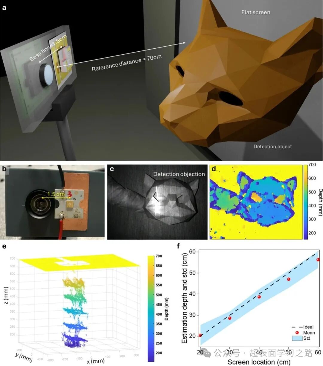
Figure 4. Single Depth Sensing Demonstration Combined with Integrated Chip and Webcam
a Single depth sensing experimental setup.
b Captured image with a hollow cat helmet.
c Corresponding depth image for (b).
d 3D point cloud for (c).
e 3D point cloud overlay of flat objects at different positions.
f Comparison curve between ideal and measured positions, verifying depth perception accuracy.
3
Summary of the Paper Update
Problem Addressed: Depth perception technology is crucial in consumer electronics, but existing dot projectors rely on bulky optical components and VCSEL arrays, resulting in large sizes (e.g., iPhone 15 is 61.25 mm³) and high power consumption. Although there are integration schemes of metasurfaces with VCSELs, they are still limited by the constraints of the 4F system focal length or require complex algorithms to reconstruct data, making it difficult to achieve chip-level monolithic integration and real-time detection.
Proposed Method: A monolithic integrated system based on GaAs photonic crystal surface-emitting laser (PCSEL) and metasurface hologram is designed, directly fabricating the metasurface on the PCSEL substrate through a non-regrowth flip-chip process. Utilizing the Γ2 band edge mode of the PhC structure achieves low-divergence beams, with the metasurface composed of a 2×2 array of square nanocolumns, optimizing phase distribution using the Gerchberg-Saxton algorithm to control the wavefront within a 19.8×19.8 μm² area, generating far-field structured light patterns without additional optical components.
Achieved Results: The device volume is only 0.025 mm³, 2450 times smaller than commercial DOE-VCSEL projectors, with a power consumption reduction of 28.7% (104.3 mW); successfully projecting random dot patterns at 70 cm and achieving depth perception, with an average standard deviation of 7.84 cm for planar object measurements, and the 3D point cloud can resolve surface indentations, validating the practical potential of the on-chip integration scheme.
Innovative Points Analysis: The first monolithic integration of metasurface with PCSEL is achieved, breaking the volume limitations of traditional 4F optical architectures, utilizing the high coherence and low divergence characteristics of the PhC mode to eliminate beam collimation components; employing propagation phase metasurface design and non-regrowth processes to avoid interference of metal contacts on laser modes while enhancing manufacturing compatibility; establishing an integrated chip paradigm of “light source-control-detection,” providing a new solution that combines miniaturization and energy efficiency for portable applications such as XR devices.
References
Monolithically Integrated Metasurface on a PCSEL for Depth Perception
Wen-Cheng Hsu, Wen-Chien Miao, Yu-Heng Hong, Hao-Chung Kuo, and Yao-Wei Huang
Nano Letters Article ASAP
10.1021/acs.nanolett.5c02540
◀
Disclaimer
▶
This public account focuses on the latest research dynamics, academic achievements, and technical applications in the field of metasurfaces. All published content and images are sourced and are for personal academic learning and knowledge accumulation only, not for commercial purposes. If you find any copyright or related issues, please contact us via email at [email protected], and we will address and coordinate the relevant matters as soon as possible.