Multisim 14 Simulation Software Analog Experiment Case: Design of a non-inverting amplifier circuit
Design Requirements: Gain of 3, verify the correctness of the circuit with input signals of both DC and AC voltages, and record the experimental results.
1. Simulation Circuit Diagram Design
(1) Double-click the NI Multisim shortcut icon on the desktop to enter the basic simulation interface, the system will automatically generate the Design1 circuit diagram file.
(2)Click on the component (Source) library, in the system default settings barFamily→POWER-SOURCES→Component→Vcc(positive power supply is 5V), click OK to place the power supply in the circuit diagram workspace; continue to selectVee(negative power supply is -5V); similarly selectGROUND for the circuit diagram ground.
(3) The working power supply voltage for the experimental chip is 15V power supply, modify the voltage value by double-clicking the power supplyVcc icon, change the voltage value to 15V, and similarly change the voltage value of the auxiliary power supplyVee to -15V.
(4)Click on the operational amplifier library, in the system default settings barFamily→OPAMP→Component→741 to place it in the circuit diagram workspace (as shown in Figure 1).
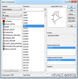
Figure 1
(5)Click on the component (Basic) library, in the system default settings barFamily→RESISTOR→Component→10K resistor, place it in the circuit diagram workspace, the experimental circuit diagram contains other resistors, you can continuously select the required resistors, such as 20K and 6.8K, you can also use the COPY command to duplicate resistors, double-click the resistor component, and modify the new resistor value in the parameter menu.
(6) Arrange the circuit diagram, to make the connections clear, flip the 741 180 degrees, click on the component 741, select (AIT+Y) to do so; if you need to modify the component symbol, double-click the component and selectLabel to modify the symbol, such as changing R1 to Rb.
(7) Point the mouse at one end of the component to see a black dot appear, press the left mouse button and drag it to another component, when another black dot appears, release the left mouse button to complete the connection, which is usually a red connection line.
2. Measure the output voltage with a DC input signal
(1) Select the experimental DC signal source, similar to the method of selecting the power supply, set Vss as the input DC voltage, and set the others to 0.1v; in the basic interface, select the digital multimeter from the virtual instrument library.
(2) Run the simulation, observe the results, and verify the correctness of the experimental design.
3. Measure the output voltage with an AC input signal
(1) Delete the measured DC power supply and multimeter, and re-select the AC-power source from the device library, double-click the component, set the parameters, change the input signal to a voltage of 1v and a frequency of 1khz AC, and select the oscilloscope from the virtual instruments (Oscilloscope).
(2) To view the output, you need to see both channels together, you can distinguish them by the color of the connections, click on the connection line to the oscilloscope, right-click and selectSegment color from the dialog box, and choose a different color.
4. Record the simulation results, and if there are issues, readjust the circuit and parameters
Run the simulation, observe the input and output waveform results using the oscilloscope. The virtual oscilloscope needs to set the Timebase and Scale to appropriate ranges, displaying 4-5 waveforms; the software defaults to a black background in the oscilloscope display window, which can be changed to white (Reverse).
The simulation circuit diagram is shown in Figure 2.
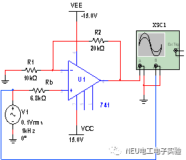
Figure 2
Multisim 14 Simulation Software Digital Experiment Case: Design a decimal counter with an initial value of 0. Design Requirements: Use 74LS161 and logic gates, design a decimal counter using the preset method, and display the output results on a seven-segment display, recording the experimental results.1. Simulation Experiment Circuit Diagram Design:
(1) Double-click the NI Multisim shortcut icon on the desktop to enter the basic simulation interface, the system will automatically generate the Design1 circuit diagram file;
(2) Click on the component (Source) library, set the chip power supply, in the system default settings barFamily→POWER-SOURCES→Component→Vcc(positive power supply is 5V), click OK to place the power supply in the circuit diagram workspace, similarly selectGROUND for the circuit ground;
(3) Click on the TTL device library, in the system default settings barFamily→74ls→Component→ 74ls161 to place it in the circuit diagram workspace, and similarly select74LS00, as shown in Figure 3;
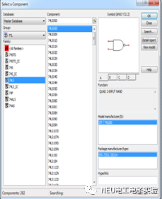
Figure 3
(4)Set the switch: click on the component (Basic) library, in the system default settings barFamily→switch→Component →STDT, place it in the circuit diagram workspace;
(5) CLOCK pulse settings: click on the component (Source) library, in the system default settings barFamily→SIGNAL-VOLTAGE-SOURCES→Component→CLOCK-VOLTAGE, click OK to place the power supply in the circuit diagram workspace, double-click the component, and modify the parameters to 1KHz;
(6) Select the output seven-segment display: click on the library, in the system default settings barFamily →HEX-DISPLAY →Component→DCD-HEX, the seven-segment display has 4 terminals, from left to right are DCBA,D is the high bit; if you want to observe high and low levels, you canPROBE to select different colors of LED lights;
(7) Arrange the circuit diagram, adjust the direction of the NAND gate as needed, click on the component 74LS00, select (AIT+X) to do so;
(8) Point the mouse at one end of the component to see a black dot appear, press the left mouse button and drag it to another component, when another black dot appears, release the left mouse button to complete the connection, which is usually a red connection line.
2. Record the simulation results, if there are issues, readjust the circuit and parameters
Run the simulation, observe the results, first verify that the initial value is 0; then verify the correctness of the experimental design, the simulation is shown in Figure 4.
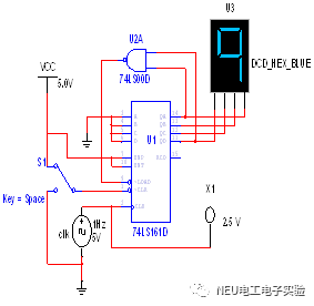
Figure 4