Skip to content
The application of push-pull circuits is very extensive, such as the push-pull mode output of microcontrollers, PWM controllers output, bridge driver circuits, etc. The English term for push-pull is: Push-Pull, which literally means push-pull. Therefore, push-pull circuits are also called push-pull type circuits.
The essence of push-pull circuits is power amplification, which enhances the driving capability of the input signal and has two characteristics:
① Very strong sinking current, that is, injecting large current into the load;
② Very strong sourcing current, that is, extracting large current from the load.
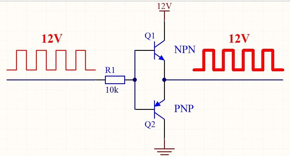
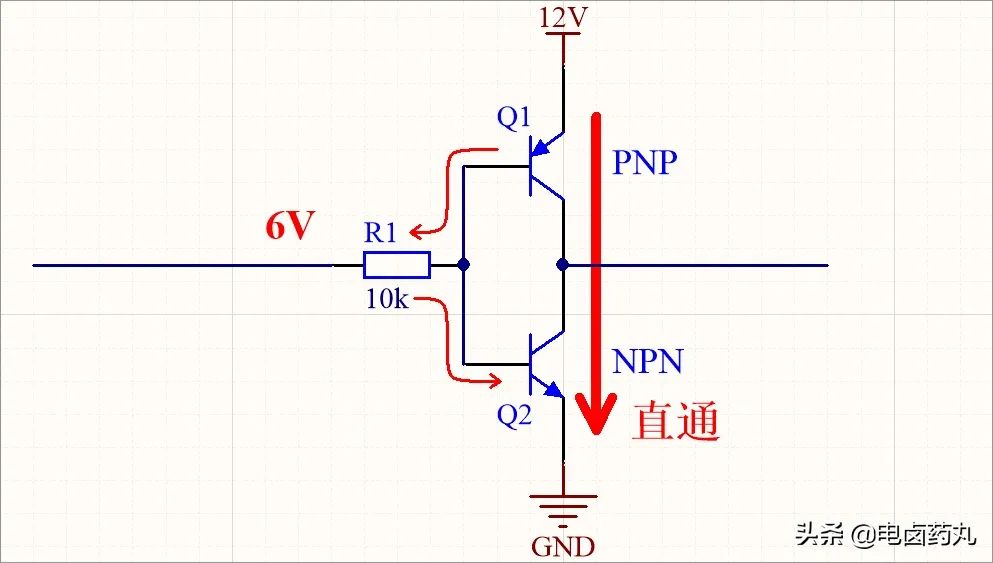
As shown in Figure 3, the push-pull circuit is composed of NPN and PNP transistors, which is our commonly used complementary push-pull circuit. Its characteristics are very low output impedance and strong driving capability.
Figure 3: Complementary Push-Pull Circuit
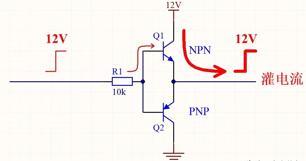
As shown in Figure 4, when the input signal jumps from low level to high level, the upper transistor turns on.
Figure 4: Upper Transistor Turned On
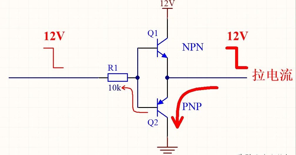
As shown in Figure 5, when the input signal jumps from high level to low level, the lower transistor turns on.
Figure 5: Lower Transistor Turned On
As shown in Figure 6, the complementary push-pull circuit formed by NPN and PNP is a common emitter output. At any moment, only one of the transistors is conducting and there is output.
Figure 6: Common Emitter Output
Some friends think that the collector (C) of the transistor is used as the output, right? Why does the circuit seem different? According to conventional thinking, it should be the circuit diagram shown in Figure 7;
If the input is 0V or 12V alone, then this circuit seems fine, but the input signal is changing, and the voltage signal has a transition process between high and low levels, so there will be a moment when both transistors conduct simultaneously at a certain intermediate voltage, which can damage the transistors, remember!
Figure 7: Incorrect Push-Pull Circuit
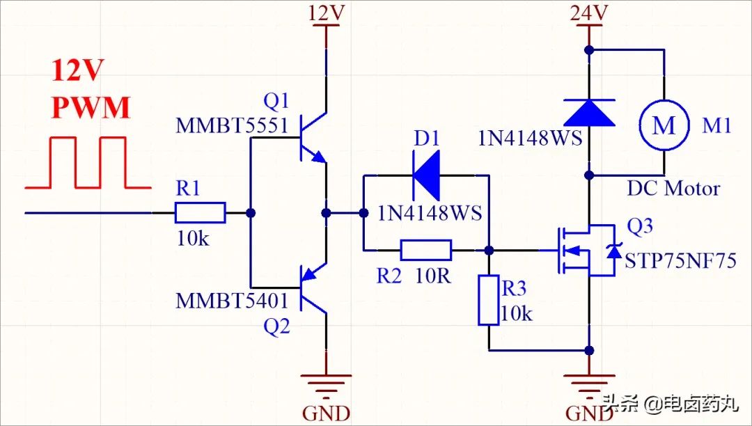
As shown in Figure 8, this is a motor speed control circuit driven by a push-pull MOSFET. The G terminal of the MOSFET has a large sinking and sourcing current, so the turn-on and turn-off times of the MOSFET are very short, and the platform voltage is also very narrow, which can effectively reduce switching losses.
Figure 8: Motor Speed Control Circuit
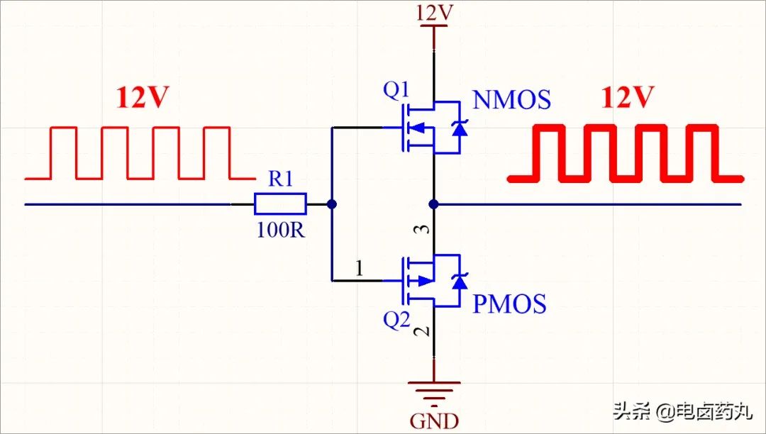
As shown in Figure 9, replacing the transistors with MOSFETs is also completely possible, and the driving capability will be stronger. (Lower PMOS body diode direction)
Figure 9: MOSFET Structure of Complementary Push-Pull
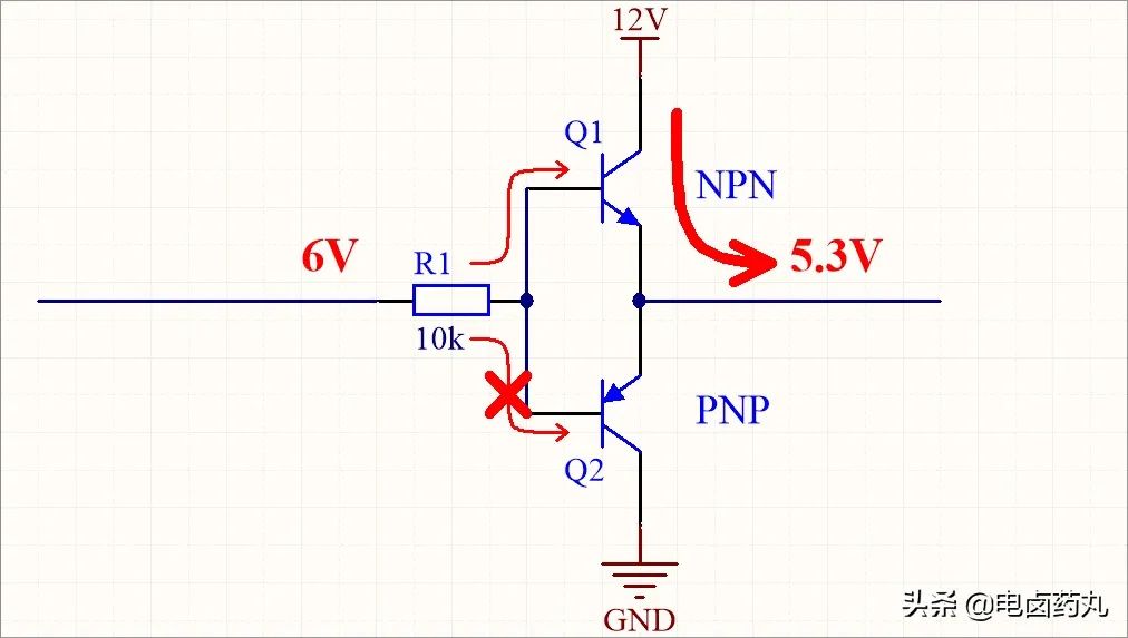
The input signal amplitude of the above complementary push-pull circuit must match the push-pull supply voltage. For example, if the push-pull supply voltage is 12V, then the amplitude of the input PWM signal must also be 12V. If the input is less than 12V, the output will also be less than 12V, as shown in Figure 6, and the voltage drop across the transistors will cause them to heat up severely. So, is there a push-pull structure that can drive a large voltage with a small voltage? Of course, there is, and it is very common in many driver chips, which we call totem pole; as shown in Figure 10.
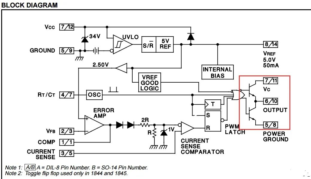
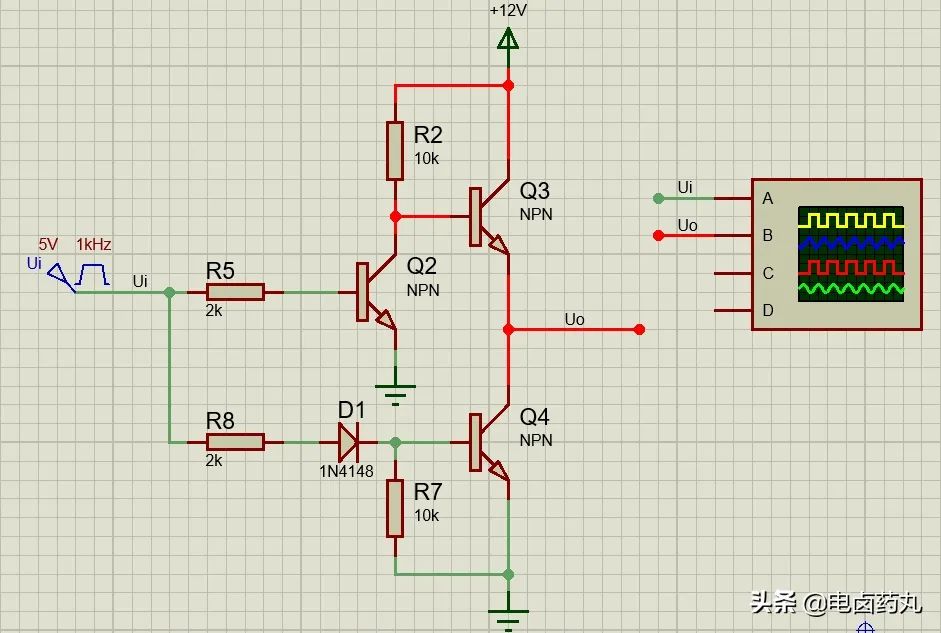
 As shown in the red box in Figure 11, the totem pole is composed of NPN and NPN, with a NOT gate in front of the upper transistor. (In fact, the chip block diagram presents some functions in a modular way, and the details involved are classified and cannot be disclosed.) Why does the chip use a totem pole instead of a complementary push-pull? The reason is that the internal operating voltage of the chip is 5V (VCC is obtained through the chip’s internal linear power supply), and from the previous analysis of the complementary push-pull, this structure is not suitable for driving large voltages with small voltages; thus, the totem pole structure was born.
As shown in Figure 12, this is the simulation circuit of the totem pole, where the signal source is a 5V/1k square wave, and the role of diode D1 is to prevent Q3 and Q4 from conducting simultaneously, which could lead to transistor damage.
Analysis: Adding a diode increases the conduction threshold voltage of the lower transistor. Before adding the diode, when the input signal is 0.7V, it turns on; after adding the diode, it requires a voltage drop of 1.4V to turn on, while the upper transistor remains at 0.7V. This is equivalent to adding a delay.
Figure 12: Totem Pole Simulation Circuit
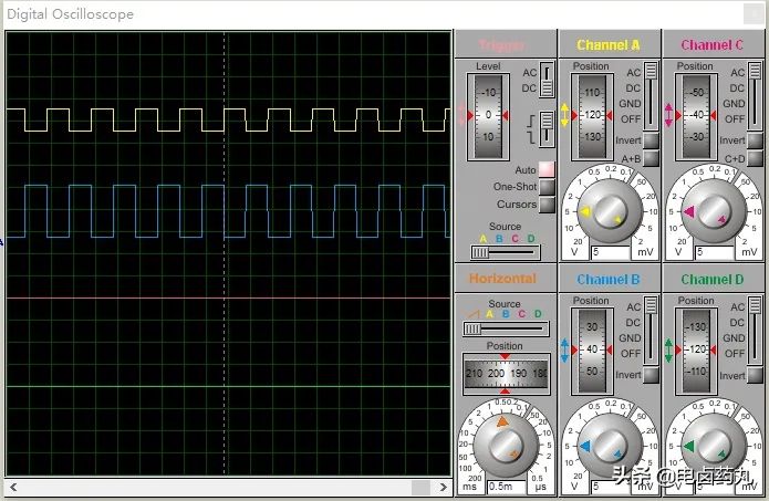
As shown in Figure 13, this is the simulation waveform of the totem pole, where the output is phase-inverted compared to the input. The yellow represents the input waveform Ui, and the blue represents the output waveform Uo, achieving small voltage driving large voltage push-pull output.
Figure 13: Totem Pole Simulation Waveform
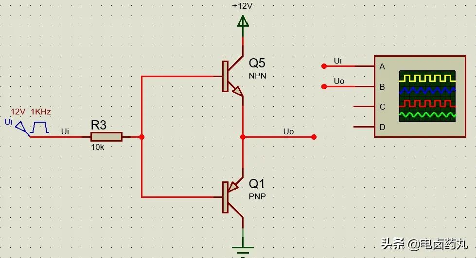
As shown in Figure 14, this is the simulation circuit of the complementary push-pull, where the signal source is a 12V/1k square wave. (Simulation software: Proteus)
Figure 14: Complementary Push-Pull Simulation Circuit
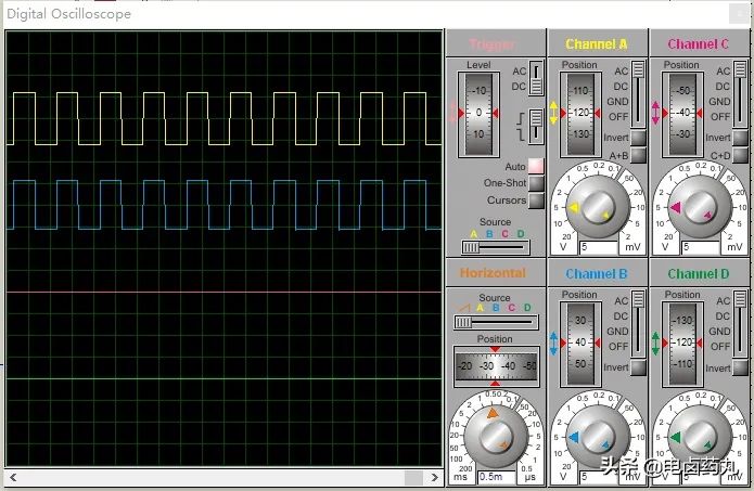
As shown in Figure 15, this is the simulation waveform of the complementary push-pull, where the output is in phase with the input. The yellow represents the input waveform Ui, and the blue represents the output waveform Uo.
Figure 15: Complementary Push-Pull Simulation Waveform
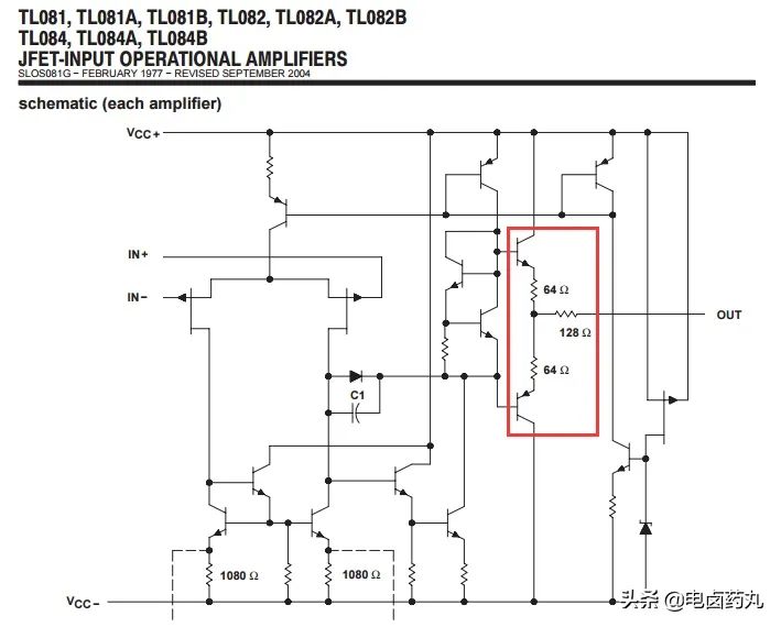
However, the operational amplifiers we commonly use also have push-pull outputs. One characteristic of operational amplifiers is that they have very high input impedance and very low output impedance, as shown in Figure 16, where the output impedance is less than 200Ω.
Figure 16: Push-Pull Output of Operational Amplifier
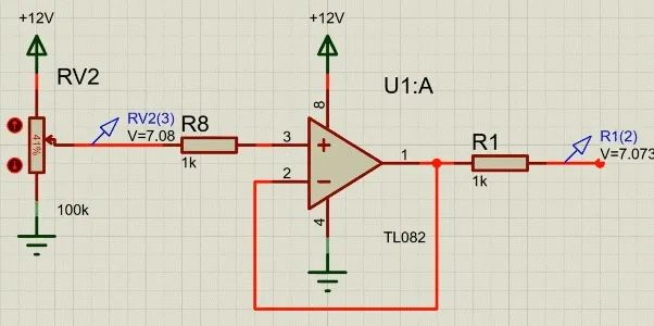
As shown in Figure 17, directly connecting the output terminal of the operational amplifier with the inverting input terminal forms a commonly used follower, where the output voltage equals the input voltage, significantly enhancing the driving capability.
① The totem pole is an NPN+NPN structure, while the complementary push-pull is an NPN+PNP structure;
② The totem pole has nonlinear characteristics and can only be used for PWM output, while the complementary push-pull has linear characteristics and can be used for both PWM output and analog signal output;
③ The totem pole is often found in PWM driver chips, used to directly drive power MOSFETs; the complementary push-pull is often found in constructed circuits as well as in MCU (microcontroller), operational amplifiers, and other chips;
④ During PWM control, the input voltage of the totem pole can be less than the driving voltage, while the complementary push-pull must have equal input and driving voltages.
Regarding the totem pole and complementary push-pull, they are often considered the same circuit (and there is controversy), but this is not the case. After correctly understanding and recognizing their differences, readers will have a new understanding of them.
Source: Toutiao / Electric Halogen Pill
As shown in the red box in Figure 11, the totem pole is composed of NPN and NPN, with a NOT gate in front of the upper transistor. (In fact, the chip block diagram presents some functions in a modular way, and the details involved are classified and cannot be disclosed.) Why does the chip use a totem pole instead of a complementary push-pull? The reason is that the internal operating voltage of the chip is 5V (VCC is obtained through the chip’s internal linear power supply), and from the previous analysis of the complementary push-pull, this structure is not suitable for driving large voltages with small voltages; thus, the totem pole structure was born.
As shown in Figure 12, this is the simulation circuit of the totem pole, where the signal source is a 5V/1k square wave, and the role of diode D1 is to prevent Q3 and Q4 from conducting simultaneously, which could lead to transistor damage.
Analysis: Adding a diode increases the conduction threshold voltage of the lower transistor. Before adding the diode, when the input signal is 0.7V, it turns on; after adding the diode, it requires a voltage drop of 1.4V to turn on, while the upper transistor remains at 0.7V. This is equivalent to adding a delay.
Figure 12: Totem Pole Simulation Circuit
As shown in Figure 13, this is the simulation waveform of the totem pole, where the output is phase-inverted compared to the input. The yellow represents the input waveform Ui, and the blue represents the output waveform Uo, achieving small voltage driving large voltage push-pull output.
Figure 13: Totem Pole Simulation Waveform
As shown in Figure 14, this is the simulation circuit of the complementary push-pull, where the signal source is a 12V/1k square wave. (Simulation software: Proteus)
Figure 14: Complementary Push-Pull Simulation Circuit
As shown in Figure 15, this is the simulation waveform of the complementary push-pull, where the output is in phase with the input. The yellow represents the input waveform Ui, and the blue represents the output waveform Uo.
Figure 15: Complementary Push-Pull Simulation Waveform
However, the operational amplifiers we commonly use also have push-pull outputs. One characteristic of operational amplifiers is that they have very high input impedance and very low output impedance, as shown in Figure 16, where the output impedance is less than 200Ω.
Figure 16: Push-Pull Output of Operational Amplifier
As shown in Figure 17, directly connecting the output terminal of the operational amplifier with the inverting input terminal forms a commonly used follower, where the output voltage equals the input voltage, significantly enhancing the driving capability.
① The totem pole is an NPN+NPN structure, while the complementary push-pull is an NPN+PNP structure;
② The totem pole has nonlinear characteristics and can only be used for PWM output, while the complementary push-pull has linear characteristics and can be used for both PWM output and analog signal output;
③ The totem pole is often found in PWM driver chips, used to directly drive power MOSFETs; the complementary push-pull is often found in constructed circuits as well as in MCU (microcontroller), operational amplifiers, and other chips;
④ During PWM control, the input voltage of the totem pole can be less than the driving voltage, while the complementary push-pull must have equal input and driving voltages.
Regarding the totem pole and complementary push-pull, they are often considered the same circuit (and there is controversy), but this is not the case. After correctly understanding and recognizing their differences, readers will have a new understanding of them.
Source: Toutiao / Electric Halogen Pill