Introduction: JTAG stands for Joint Test Action Group, which is commonly referred to in the IEEE standard 1149.1 as the Standard Test Access Port and Boundary Scan Architecture. Its functionality is powerful, but for engineers engaged in embedded development, the most frequently used feature is programming chips, which typically requires a dedicated emulator. This article teaches you how to eliminate the emulator and significantly improve debugging convenience.Main Content:1. JTAG Interface of FPGA As seen in UG470, the FPGA has reserved a standard JTAG interface and has drawn a 14-pin JTAG connector, essentially recommending its own emulator.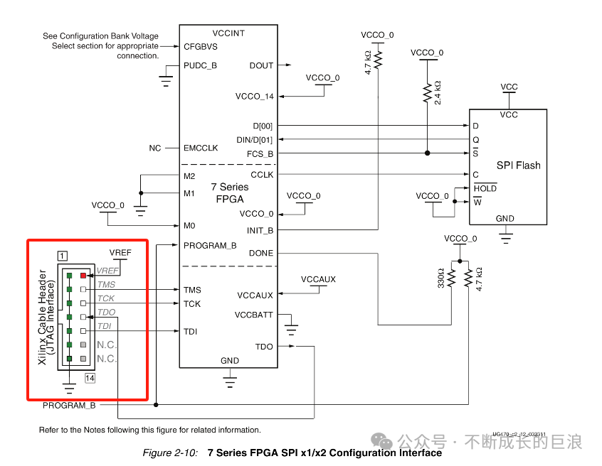 JTAG includes four signals: TDI (Test Data Input), TDO (Test Data Output), TMS (Test Mode Select), and TCK (Test Clock). It is also important to note the value of Vref, which is a reference voltage provided to the JTAG emulator, usually set equal to VCCAUX. TDI and TDO can be connected to other devices, such as PROM, by connecting the TDO of the current stage to the TDI of the next stage, and the TDO of the last stage device returns to the TDO pin on the JTAG socket. This way, a single emulator can scan all devices, as shown in the figure below.
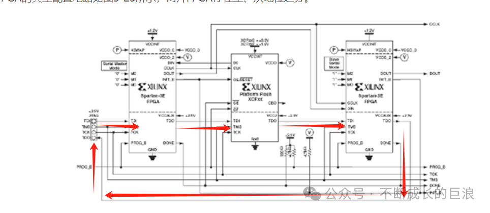 Generally, to debug an FPGA, you need such an emulator, which costs around a thousand yuan. One end connects to your computer’s USB port, and the other end connects to the FPGA emulator terminal.
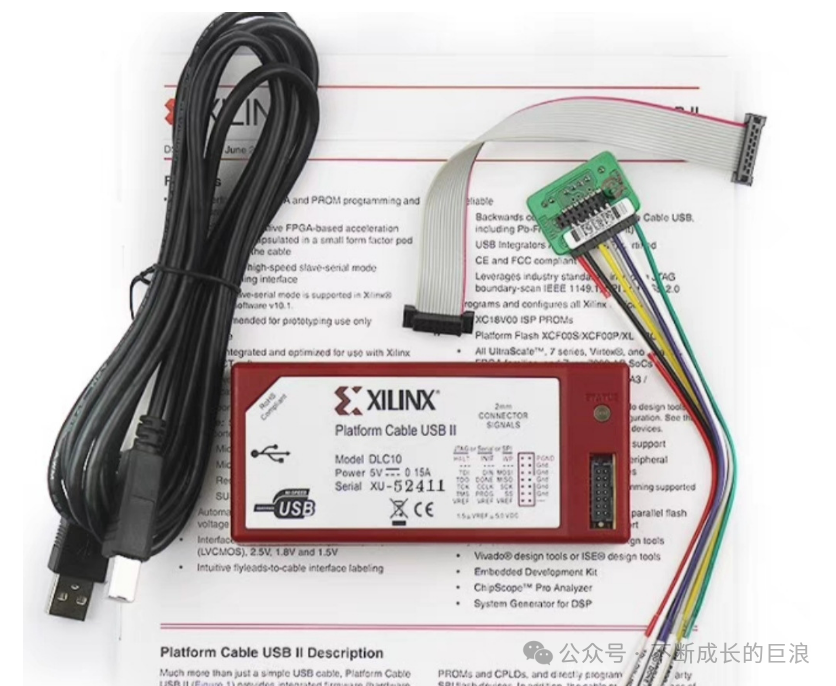 This is the standard practice, and currently, 80% of engineers still use this solution. However, there are several drawbacks: first, the high cost of the emulator; second, the inconvenience of carrying it around for debugging; and third, the cables can easily get damaged over time. Thus, clever engineers have been wondering if it is possible to complete debugging with just a mobile phone cable in this day and age. The answer is yes, but it requires additional circuitry. Please see the next section. 2. USB to JTAG Circuit We can use a chip that converts JTAG signals to USB signals, and then output the USB signals to a USB socket, allowing us to start debugging happily with just a mobile phone charging cable. There are two common chip solutions: one is the FTDI company’s FT232H/FT2232H series. Both FT232H and FT2232H support USB 2.0 high-speed mode (480Mbps) and full-speed mode (12Mbps), and both have an integrated MPSSE (Multi-Protocol Synchronous Serial Engine), supporting various communication protocols such as JTAG, I2C, and SPI. The FT2232H has an additional channel compared to the FT232H.
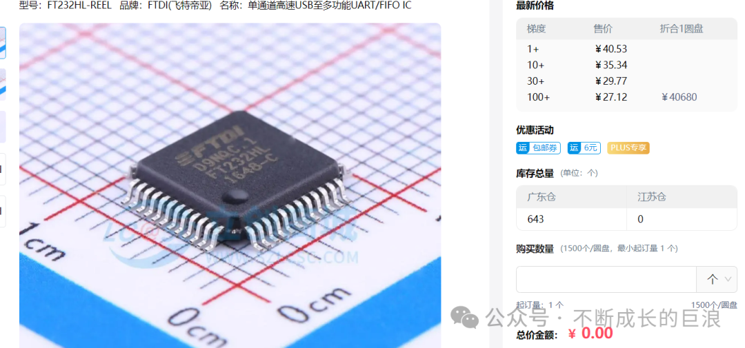 FTDI produces corresponding modules with USB-MiniB interfaces, but in the era of rapidly proliferating Type-C mobile phone cables, these data cables still need to be purchased separately, which is inconvenient.
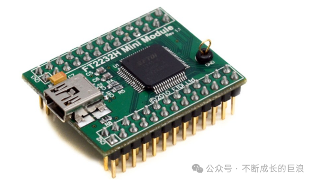 So, are there modules with Type-C interfaces? I just want to carry my computer and mobile phone data cable, nothing else!
 Browsing through a certain treasure, I was not disappointed; there are many manufacturers, but the solutions are similar, and the prices are all under 100 yuan, much cheaper than buying any counterfeit emulator.
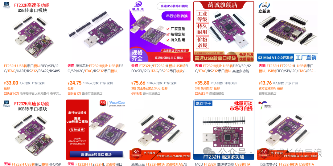 We can leave pin holes on our designed baseboard, solder the purchased module onto it, and then follow the programming method provided by the manufacturer to use it normally. Alternatively, to further improve integration and achieve technological independence, we can directly build the peripheral circuitry of the chip on the baseboard. It is important to note that the FT232H chip requires an external crystal oscillator to provide the working clock, the voltage levels of FT232 must match the JTAG signals, and an EEPROM is needed to store the program, which must be installed and programmed before use. Our domestic chip manufacturers also have related solutions; for example, Nanjing Qinheng’s conversion chip CH347 does not require an external storage chip, as it has built-in programs, eliminating the need for programming steps and improving efficiency. Let’s give a thumbs up to domestic products.
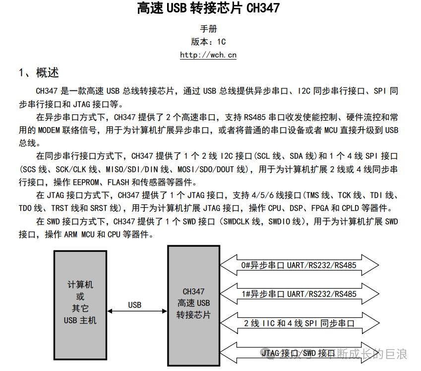 The two solutions mentioned above, the FTDI chip integrated solution, have been used in bulk in the author’s company’s products, and the results are very good, with no difference from debugging with an emulator. Colleagues working with FPGAs have even bought the author milk tea. During the usage process, some issues were encountered and resolved. If you encounter problems during use, feel free to leave a message or contact me for communication. The domestic chip solution has not been tried yet, but I hope to try it in the future. The following post contains some experiences of use, which you can refer to; there should still be some issues, so caution is advised for bulk product usage.https://zhuanlan.zhihu.com/p/566454129Conclusion: In this issue, we introduced a very practical USB to JTAG circuit, liberating engineers from emulator boxes. If you are interested in the hardware circuit diagram or have any issues during use, feel free to communicate with me.In closing: I have been busy with work recently, and the update frequency has noticeably slowed down. I have followed many high-quality and excellent authors, but in the end, they all stopped updating indefinitely, which is very regrettable. I hope to receive everyone’s support to continue and produce high-quality content.This resource is for learning and communication purposes only and is strictly prohibited for commercial use.I hope everyonelikes,shares, saves, comments, and appreciates to encourage more updates.