1. Introduction to A/D Converters
An A/D converter (ADC) converts analog signals into digital signals, allowing microcontrollers to process data. With the rapid development of large-scale integrated circuit technology, a variety of A/D conversion chips with different structures and performances have emerged.
1. Overview of A/D Converters
Currently, there are many single-chip ADCs available, and designers only need to make reasonable chip selections. Some microcontrollers now integrate A/D converters with resolutions of 8, 10, or 12 bits, and they also have fast conversion speeds. However, when the on-chip A/D converters do not meet the requirements, external expansion is still necessary. Therefore, mastering the basic methods of using external A/D converters is essential.
Although there are many types of A/D converters, the most widely used in microcontroller application systems are the successive approximation type and the dual-slope type converters.
The successive approximation A/D converter is the most commonly used A/D converter, offering a balance of accuracy, speed, and cost. The dual-slope A/D converter has advantages such as high accuracy, good anti-interference capability, and low cost, but it has a slower conversion speed compared to the successive approximation type. In recent years, it has been widely used in microcontroller applications.
A/D converters are classified based on the effective number of output bits into various types, including 4-bit, 8-bit, 10-bit, 12-bit, 14-bit, and 16-bit parallel outputs, as well as BCD code outputs of 3.5-bit, 4.5-bit, and 5.5-bit. Currently, in addition to parallel A/D converters, the use of A/D converters with synchronous SPI serial interfaces is also increasing. Serial interface A/D converters have advantages such as occupying fewer microcontroller port lines, ease of use, and simple interfaces, and they have been widely adopted. Typical serial A/D converters include TI’s TLC549 (8-bit), TLC1549 (10-bit), TLC1543 (10-bit), and TLC2543 (12-bit).
A/D converters can be roughly classified by conversion speed into ultra-high speed (conversion time ≤ 1ns), high speed (conversion time ≤ 1µs), medium speed (conversion time ≤ 1ms), and low speed (conversion time ≤ 1s). Many new types of A/D converters have integrated multiplexers, clock circuits, reference voltage sources, binary/decimal decoders, and conversion circuits into a single chip, providing great convenience for users.
2. Main Technical Specifications of A/D Converters
(1) Conversion time or conversion rate. Conversion time refers to the time required for an A/D converter to complete one conversion. The reciprocal of conversion time is the conversion rate.
(2) Resolution. Resolution is a technical specification that measures the smallest change in the input analog signal that the A/D converter can distinguish. Resolution depends on the number of bits of the A/D converter, and is typically expressed in terms of the number of output binary bits. For example, a certain model of A/D converter has a full-scale input voltage of 5V and can output a 12-bit binary number, quantifying the input using 212 values, with a resolution of 1 LSB, which is 5V/212=1.22mV. Its resolution is 12 bits, meaning it can distinguish changes in input voltage of 1.22mV. However, for the dual-slope BCD output A/D converter MC14433, when the full-scale conversion voltage is set to 2V, its output decimal range is 0000 to 1999, allowing it to distinguish changes of 1mV. If the resolution is converted to binary bit representation, a 3.5-bit A/D converter (where the thousands place has only two decimal digits, 0 and 1, referred to as half a bit, while the hundreds, tens, and units places can have 10 decimal digits from 0 to 9, referred to as three complete bits) has a resolution of approximately 11 bits, since 1999 is closest to 2 raised to the power of 11 = 2048.
The error caused by the quantization process is known as quantization error. Quantization error arises from the quantization of the analog signal by a finite number of digital values. Theoretically, quantization error is defined as ± 1/2 LSB of one unit of resolution. Increasing the number of bits in the A/D converter can improve resolution and reduce quantization error.
(3) Conversion accuracy. This is defined as the difference between an actual A/D converter and an ideal A/D converter in terms of quantized values, which can be expressed as absolute or relative error.
2. Overview of ADC0809
1. Functions and Pins of ADC0809
The ADC0809 is a successive approximation type A/D converter with 8 analog input channels and 8-bit parallel digital output. Its pin configuration is shown in Figure 1.
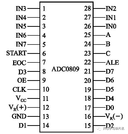
Figure 1: Pin Diagram of ADC0809
It has a total of 28 pins in a dual in-line package.
The pin functions are as follows:
IN0 to IN7: 8 analog signal input terminals.
D0 to D7: 8-bit digital output terminals after conversion.
A, B, C, and ALE: Control the switching of the 8 analog input channels. A, B, and C are connected to three address lines of the microcontroller, with the three-bit code corresponding to the addresses of the 8 channel ports. The codes C, B, A = 000 to 111 correspond to the addresses of channels IN0 to IN7. Switching between the analog inputs is achieved by changing the codes on pins C, B, and A through software.
OE, START, CLK: OE is the output enable pin, START is the start signal input pin, and CLK is the clock signal input pin.
EOC: End of conversion signal. This pin is low when the A/D conversion starts and goes high when the A/D conversion ends.
VR(+), VR(-): Reference voltage input terminals.
2. Interface Design between Microcontroller and ADC0809
When the microcontroller reads the conversion results from the ADC, it can use either polling or interrupt control methods.
The polling method involves the microcontroller sending the start signal to the ADC and then executing other programs while continuously checking the EOC pin of the ADC0809 to see if the conversion has completed. Once the conversion is complete, the microcontroller reads the converted data.
The interrupt control method involves the microcontroller sending the start signal to the ADC and then executing other programs. When the ADC0809 finishes conversion and sends an interrupt request signal to the microcontroller, the microcontroller responds to this interrupt request, enters the interrupt service routine, and reads the converted data.
The interrupt control method is more efficient, making it particularly suitable for ADCs with longer conversion times.