
Continuing from the previous article, a typical low power design in digital chips is the addition of a clock gate. Another method is through parallel and pipelining techniques.
Parallel and Pipelining
The prominent advantage of hardware description languages is the parallelism in instruction execution. Multiple statements can process several signal data in parallel within the same clock cycle. However, when data is input serially, the advantages of parallel instruction execution are not realized. Moreover, many computations cannot be completed within one or two clock cycles. If each serial data input must wait for the previous computation to finish before starting the next computation, the efficiency is significantly low. Pipelining addresses the issue of low efficiency in serial data computation over multiple cycles. Generally, a functional module can be implemented either in parallel or through pipelining; both methods trade resources for speed.
For parallel processing, multiple execution statements can be processed simultaneously, increasing execution efficiency. Under the premise of meeting design specifications, parallel processing can reduce the clock frequency, thereby achieving lower power consumption. For example, if implementing 4 data multiply-accumulate operations, it can be done using 1 multiplier or through 2 multipliers (in parallel). The Verilog code descriptions are as follows:
//1 multiplier, high speed
module  mul1_hs    (
        input           clk ,           //200MHz
        input           rstn ,
        input           en  ,
        input [3:0]     mul1 ,          //data in
        input [3:0]     mul2 ,          //data in
        output          dout_en ,
        output [8:0]    dout     );
    reg                  flag ;
    reg                  en_r ;
    always @(posedge clk or negedge rstn) begin
        if (!rstn) begin
            flag   <= 1'b0 ;
            en_r   <= 1'b0 ;
        end
        else if (en) begin
            flag   <= ~flag ;
            en_r   <= 1'b1 ;
        end
        else begin
            flag   <= 1'b0 ;
            en_r   <= 1'b0 ;
        end
    end
    wire [7:0]           result = mul1 * mul2 ;
    // data output en
    reg [7:0]            res1_r, res2_r ;
    always @(posedge clk or negedge rstn) begin
        if (!rstn) begin
            res1_r         <= 'b0 ;
            res2_r         <= 'b0 ;
        end
        else if (en && !flag) begin
            res1_r         <= result ;
        end
        else if (en && flag) begin
            res2_r         <= result ;
        end
    end
    assign dout_en = en_r && !flag ;
    assign dout = res1_r + res2_r ;
endmodule
//===========================================
// 2 multiplier2, low speed
module  mul2_ls    (
        input           clk ,           //100MHz
        input           rstn ,
        input           en  ,
        input [3:0]     mul1 ,          //data in
        input [3:0]     mul2 ,          //data in
        input [3:0]     mul3 ,          //data in
        input [3:0]     mul4 ,          //data in
        output          dout_en,
        output [8:0]    dout     );
    wire [7:0]           result1 = mul1 * mul2 ;
    wire [7:0]           result2 = mul3 * mul4 ;
    //en delay
    reg                  en_r ;
    always @(posedge clk or negedge rstn) begin
        if (!rstn) begin
            en_r           <= 1'b0 ;
        end
        else begin
          en_r           <= en ;
        end
    end
    // data output en
    reg [7:0]            res1_r, res2_r ;
    always @(posedge clk or negedge rstn) begin
        if (!rstn) begin
            res1_r         <= 'b0 ;
            res2_r         <= 'b0 ;
        end
        else if (en) begin
            res1_r         <= result1 ;
            res2_r         <= result2 ;
        end
    end
    assign dout          = res1_r + res2_r ;
    assign dout_en       = en_r ;
endmodule
The testbench description is as follows:
`timescale 1ns/1ps
module test ;
    reg          rstn ;
    //mul1_hs
    reg          hs_clk;
    reg          hs_en ;
    reg [3:0]    hs_mul1 ;
    reg [3:0]    hs_mul2 ;
    wire         hs_dout_en ;
    wire [8:0]   hs_dout ;
    //mul1_ls
    reg          ls_clk = 0;
    reg          ls_en ;
    reg [3:0]    ls_mul1 ;
    reg [3:0]    ls_mul2 ;
    reg [3:0]    ls_mul3 ;
    reg [3:0]    ls_mul4 ;
    wire         ls_dout_en ;
    wire [8:0]   ls_dout ;
    //clock generating
    real         CYCLE_200MHz = 5 ; //
    always begin
        hs_clk = 0 ; #(CYCLE_200MHz/2) ;
        hs_clk = 1 ; #(CYCLE_200MHz/2) ;
    end
    always begin
        @(posedge hs_clk) ls_clk = ~ls_clk ;
    end
    //reset generating
    initial begin
        rstn      = 1'b0 ;
        #8 rstn      = 1'b1 ;
    end
    //motivation
    initial begin
        hs_mul1   = 0 ;
        hs_mul2   = 16 ;
        hs_en     = 0 ;
        #103 ;
        repeat(12) begin
            @(negedge hs_clk) ;
            hs_en          = 1 ;
            hs_mul1        = hs_mul1 + 1;
            hs_mul2        = hs_mul2 - 1;
        end
        hs_en = 0 ;
    end
    initial begin
        ls_mul1   = 1 ;
        ls_mul2   = 15 ;
        ls_mul3   = 2 ;
        ls_mul4   = 14 ;
        ls_en     = 0 ;
        #103 ;
        @(negedge ls_clk) ls_en = 1;
        repeat(5) begin
            @(negedge ls_clk) ;
           ls_mul1        = ls_mul1 + 2;
           ls_mul2        = ls_mul2 - 2;
           ls_mul3        = ls_mul3 + 2;
           ls_mul4        = ls_mul4 - 2;
        end
        ls_en = 0 ;
    end
    //module instantiation
    mul1_hs    u_mul1_hs    (
      .clk              (hs_clk),
      .rstn             (rstn),
      .en               (hs_en),
      .mul1             (hs_mul1),
      .mul2             (hs_mul2),
      .dout             (hs_dout),
      .dout_en          (hs_dout_en)
    );
    mul2_ls    u_mul2_ls    (
      .clk              (ls_clk),
      .rstn             (rstn),
      .en               (ls_en),
      .mul1             (ls_mul1),
      .mul2             (ls_mul2),
      .mul3             (ls_mul3),
      .mul4             (ls_mul4),
      .dout             (ls_dout),
      .dout_en          (ls_dout_en)
    );
    //simulation finish
    always begin
        #100;
        if ($time >= 1000)  begin
            #1 ;
            $finish ;
        end
    end
endmodule
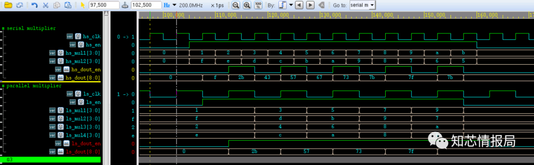
The simulation results are shown below. The results of the two implementation methods are the same, but for the parallel processing method, since its clock frequency is reduced by 1/2, the power consumption will also decrease, although the circuit area will increase.
For a continuous operation mode N-stage pipeline, the efficiency improves by N times. Similar to parallel design, pipelining design can also achieve lower power consumption by reducing the operating frequency. Additionally, we can divide the pipelining design into N stages. Assuming the new path length is Lnew and the original path length is Lold, then Lnew=1/N*Lold. If the clock frequency remains fixed, then within one cycle, it is not necessary to charge and discharge the original capacitance C, but only to charge and discharge the capacitance C/N. Therefore, a lower voltage can be used to drive the chip circuit, thus achieving lower power consumption.
Resource Sharing and State Encoding
For a design where the same logic is called in multiple places, resource sharing can be implemented to reduce power consumption. For example, for a comparison logic, the code description without resource sharing is as follows:
always @(*) begin
        case (mode) :
            3'b000:         result  = 1'b1 ;
            3'b001:         result  = 1'b0 ;
            3'b010:         result  = value1 == value2 ;
            3'b011:         result  = value1 != value2 ;
            3'b100:         result  = value1 > value2 ;
            3'b101:         result  = value1 < value2 ;
            3'b110:         result  = value1 >= value2 ;
            3'b111:         result  = value1 <= value2 ;
        endcase    end
After improvement, the code description using resource sharing is as follows:
    wire equal_con       = value1 == value2 ;
    wire great_con       = value1 > value2 ;
    always @(*) begin
        case (mode) :
            3'b000:         result  = 1'b1 ;
            3'b001:         result  = 1'b0 ;
            3'b010:         result  = equal_con ;
            3'b011:         result  = equal_con ;
            3'b100:         result  = great_con ;
            3'b101:         result  = !great_con && !equal_con ;
            3'b110:         result  = great_con && equal_con ;
            3'b111:         result  = !great_con ;
        endcase    end
In the first method, if the compiler optimization is not done well, it may require 6 comparators. The second resource sharing method only requires 2 comparators to achieve the same logical function, thus reducing power consumption to some extent.
For some frequently changing signals, the toggle rate is relatively high, leading to higher power consumption. State encoding can be utilized to reduce switching activity and decrease power consumption. For example, when a high-speed counter operates, using Gray code instead of binary encoding results in only 1 bit of data toggling at any moment, reducing the toggle rate and consequently the power consumption. Similarly, in state machine design, if the state encoding before and after switching has only a 1-bit difference, it will also reduce the toggle rate.
Operand Isolation
Operand isolation refers to the situation where, during operations such as selection, if we know that the selected option isA and notB, then a lot of calculations forB become unnecessary. Therefore, operand isolation involves adding some selection devices so that if an operand is not needed, it is not selected, and the calculations required for that operand are not performed.Without operand isolation, the Verilog code description is as follows:
module isolated(A,B,C,D,clk,clr,choose,result);
input wire clk;
input wire clr;
input wire [1:0]choose;
input wire [31:0]A;
input wire [31:0]B;
input wire [31:0]C;
input wire [31:0]D;
output reg [31:0]result;
wire [31:0]choose_a;
wire [31:0]choose_b;
wire [31:0]choose_c;
wire [31:0]choose_d;
//This is a simple mux, first calculate the values of A, B, C, D and then select
assign choose_a = A*B;
assign choose_b = A+B+C+D;
assign choose_c = B*C;
assign choose_d = C*D;
always@(posedge clk,posedge clr)begin
   if(clr) result <= 0;else  begin
  if(choose == 2'b00)  result <= choose_a;else if(choose == 2'b01)  result <= choose_b;else if(choose == 2'b10)  result <= choose_c;else  result <= choose_d;
end
end
endmodule
Using operand isolation, the Verilog code description is as follows:
module isolated2(A,B,C,D,clk,clr,choose,result);
input wire clk;
input wire clr;
input wire [1:0]choose;
input wire [31:0]A;
input wire [31:0]B;
input wire [31:0]C;
input wire [31:0]D;
output reg [31:0]result;
reg [31:0]choose_A;
reg [31:0]choose_B;
reg [31:0]choose_C;
reg [31:0]choose_D;
reg [1:0]cho;//This is a mux using isolated, first calculate the required A, B, C or D values based on the signal
always@(posedge clk,posedge clr)begin
   if(clr)  begin
         choose_A <= 0;
         choose_B <= 0;
         choose_C <= 0;
         choose_D <= 0;
cho      <= 0;
endelse if(choose == 2'b00)  begin
         choose_A <= A;
         choose_B <= B;
         choose_C <= choose_C;
         choose_D <= choose_D;
cho      <= 0;
endelse if(choose == 2'b01)  begin
         choose_A <= A;
         choose_B <= B;
         choose_C <= C;
         choose_D <= D;
cho      <= 1;
endelse if(choose == 2'b10)  begin
         choose_A <= choose_A;
         choose_B <= B;
         choose_C <= C;
         choose_D <= choose_D;
cho      <= 2;
endelse  begin
         choose_A <= choose_A;
         choose_B <= choose_B;
         choose_C <= C;
         choose_D <= D;
cho      <= 3;
end
end
always@(posedge clk,posedge clr)begin
   if(clr) result <= 0;else   begin
  if(cho == 2'b00)  result <= choose_A*choose_B;else if(cho == 2'b01)   result <= choose_A+choose_B+choose_C+choose_D;else if(cho == 2'b10)    result <= choose_B*choose_C;   else    result <= choose_C*choose_D;
end
end
endmodule
References:https://www.runoob.com/w3cnote/verilog2-rtl-low-power-design-1.html
The content of this article represents the author’s views and does not reflect the views of the platform.
If there are any objections, please feel free to contact us.
If there is any infringement, please contact us for deletion.
PreviousHighlightsReview
The first snow of 2021! Interpretation of Intel’s Q4 2020 financial report
Lossless compression efficiency of JPEG-LS, PNG, QOI, and JPEG2000: A comparative study

Technological advancements in core IP accelerate innovation in satellite navigation chips

The semiconductor law is gradually failing; what does the future hold for processors?