
1. Concept
Composition of Power Consumption: Three main sources of power consumption: surge, static power, and dynamic power;
Surge Current:
Refers to the maximum instantaneous input current generated when the device is powered on, known as the inrush current; The surge current is device-dependent;
Surge power is not our primary concern, so it is only mentioned to indicate its existence.
Static Power Consumption: Also known as standby power, static power consumption is mainly caused by the leakage current of transistors;
Dynamic Power Consumption: Includes switching power or flip power, short-circuit power or internal power.
Factors Affecting Dynamic Power Consumption: Gate parasitic capacitance, clock toggle rate, clock frequency, supply voltage;
Reducing Power Consumption: Should be addressed at all design levels, namely system level, logic level, and physical level, with higher levels being more effective in reducing power consumption;
Maximum reduction can be achieved at the system and architecture levels;
2. Low Power Technologies
2.1 System-Level Power Reduction Techniques:
-
System on Chip Approach
-
Hardware/Software Partitioning: Simulating and modeling system performance to determine which parts should be implemented in hardware and which in software, achieving an optimal balance between performance and power consumption
-
Using Low Power Software
-
Choosing the Right Processor
2.2 Architecture-Level Power Reduction Techniques:
-
Multi-Voltage Design Technology (Multi-VDD:
Includes Voltage Control Unit:
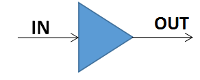
Level shifters: Converts signals from high (low) voltage regions to low (high) voltage regions. Signals typically include data, clock, scan chain data, etc. The schematic of a level shifter is shown below:
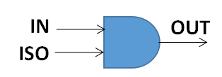
Power isolation cell: Mainly used for module input and output. It can hold the signal constant when the power is turned off, thus avoiding floating inputs in the unit. The power isolation cell is shown below:
Retention register: Keeps the state of the register when not in operation.
-
Advanced Clock Gating: Using gated clock signals
-
Dynamic Voltage Frequency Scaling (DVFS): Reducing clock speed and supply voltage
-
Cache-Based System Architecture: Using small range caches
-
Logarithmic FFT Architecture: Implementing FFT based on logarithmic systems
-
Asynchronous (Clockless) Design: Removing the clock
-
Power Gating: (Static Power) Refers to turning off the power supply to a certain area of the chip, disconnecting the power supply to the logic circuits in that area (turning it off when the module is not in use) to minimize leakage current; high threshold voltage cells are often used for gated power transistors;
-
High Threshold Voltage (HV): Increasing the threshold voltage can reduce leakage current;
-
Memory Power Gating: Turning off memory when not in use (Static Power)
2.3 RTL Level Power Reduction:
-
Parallelism and Pipelining:: Using parallel processing can reduce the system operating frequency, thereby potentially lowering power consumption.
-
State Machine Encoding and Decoding:: Gray code is most suitable for low power design, as Gray code has fewer transitions than binary code, which can reduce switching activity and lower power consumption.
-
Clock Gating::
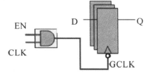
In the above circuit diagram, the control signal (EN) is directly ANDed with the clock signal (CLK) to complete the gating. The gated clock signal GCLK is sent to the register, and when EN is 0, the clock is turned off.
Without using clock gating:
always@(posedge clock or negedge reset_b) if(!reset_b) test_ff <= 32'b0; else test_ff <= test_nxt;assign test_nxt = load_cond ? Test_data : test_ff;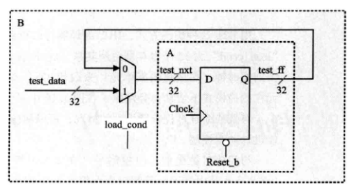
Using clock gating:
always@(posedge clock or negedge reset_b) if(!reset_b) test_ff <= 32'b0; else if(load_cond) test_ff <= test_data;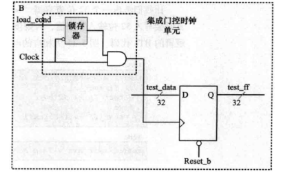
-
One-Hot Code Multiplexer: One-hot encoding is faster and more stable than binary encoding, allowing unselected buses to be masked early to achieve low power effects;
Binary encoding for MUX selection:
case (SEL) 2'b00: OUT = a; 2'b01: OUT = b; 2'b10: OUT = c; 2'b11: OUT = d; endcase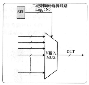
MUX selection using binary encoding
MUX selection using one-hot encoding:
case (SEL) 4'b0001: OUT = a; 4'b0010: OUT = b; 4'b0100: OUT = c; 4'b1000: OUT = d; default: OUT = 'X'; endcase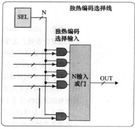
MUX selection using one-hot encoding
-
Eliminating Excess Transitions
-
Resource Sharing: Resource sharing reduces power consumption; if the same operation is used in multiple places, it can avoid repeating the same computational logic in multiple locations.
-
Using Wave Counters to Reduce Power Consumption: Can reduce leakage current and lower power consumption, but must be used with caution.
-
Bus Transition Encoding Technique: If the Hamming distance between the current data and the next data is greater than N/2 (where N is the bus width), the next data is output in reverse to reduce the number of transitions on the bus; this is very effective for reducing transitions on large buses;
-
High Activity Networks:: Distinguishing between high and low activity networks and placing them as deep as possible in the logic cloud;
-
Enable and Disable Logic: Cloud
2.4 Physical Level Low Power Techniques
-
Technology Level: Further reducing power consumption through advanced silicon processing technology;
-
Layout Optimization: Optimizing wiring, as long wiring increases power consumption
-
Substrate Bias: Also known as reverse bias, can reduce leakage power consumption
-
Reducing Oxide Layer Thickness:
-
Multiple Oxide Layer Thickness:
-
Design to Reduce Capacitance:
-
For nodes with frequent toggling activity in the design, use low-capacitance metal layers for wiring;
-
Keep high toggle rate nodes as short as possible;
-
For high-load nodes and buses, use low-capacitance metal layers;
-
For particularly wide devices, use special layout techniques to achieve smaller drain junction capacitance.
-
In some layout tools, power consumption can be set as an optimization target for generating clock trees.
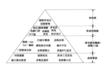
Power Reduction Techniques at Various Levels
[A Written Test Question]
1. Which of the following power reduction measures can lower peak power?
A Static Module Level Clock Gating
B Memory Shut Down
C Power Gating
D Significantly Increasing HVT Ratio
Analysis: First, peak power belongs to the short-circuit power in dynamic power consumption, which is caused by both NMOS and PMOS being on simultaneously, resulting in peak current and ultimately power consumption. This power consumption is related to supply voltage, clock toggle rate, and peak current.
Option A is static clock gating, so option A is incorrect.
Option B is memory shut down. That is, when not accessed, the memory is turned off, thus also reducing static power consumption.
Option C is power gating technology, which means turning off the power when the module is not working, putting the module to sleep, and then turning on the power again when it works, which reduces static power consumption.
Option D means using high threshold voltage transistors, the effect of increasing threshold voltage is to reduce sub-threshold leakage current, and the short-circuit power formula is: Pshort = τAshortVdd = τAβ(Vdd-Vth)³, which is only related to Vth. In option D, significantly increasing HVT (High Voltage Value) will reduce short-circuit power, thus lowering peak power in dynamic power consumption. Therefore, option D is correct.
2. In low power design of logic circuits, which method is ineffective?
A Using Slow Design
B Reducing Signal Transitions
C Using Slower Clock
D Increasing Threshold Voltage
Analysis: Option A states that using slow design does not necessarily reduce power consumption, so option A is incorrect.
Option B reduces signal transitions, which can lower dynamic power consumption.
Option C using a slower clock also relatively reduces signal transitions, thus also lowering dynamic power consumption.
Option D means using high threshold voltage transistors, the effect of increasing threshold voltage is to reduce sub-threshold leakage current, thus lowering static power consumption.
3. In the RTL design phase, common design methods to reduce power consumption are:
A Gate-Level Circuit Power Optimization
B Clock Gating
C Reducing Circuit Leakage Current
D Multi-Threshold Voltage
Analysis: All four options are common design methods to reduce power consumption, but there is a premise, which is that in the RTL design phase, that is, the stage where we can control when writing code, we can add clock gating in the code, so option B is correct.
4. In a certain state, if the output value of a certain register is not concerned, then designing it to output 0 can reduce power consumption (Incorrect)
Analysis: Compared to designing it to output 0, a better way to reduce power consumption is to keep the register’s original value. Because power consumption comes from signal toggling, if the previous state of the register output is 1, and the next state output is 0, even if 0 is not used, it still generates a transition from 0 to 1, which will also consume power. Since it is not concerned, it is better to keep the output as 1.
5.Isolation cell is which of the following low power technologies necessary for?
A. Clock gating
B. Multi VDD
C. Power gating
D. Multi VT
Analysis: As introduced above
6. Which of the following is not a basic factor affecting chip power consumption:
Voltage Temperature Process Humidity