Skip to content
 【Do you often design PCBs? Scan the code to reply “PCB” and join our practical series group on the topic of “PCB Design”】
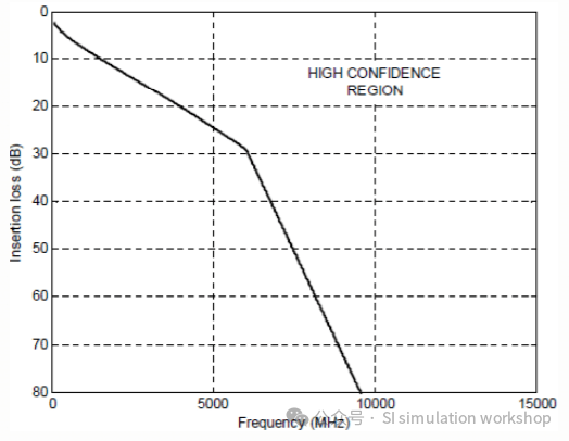
From a system design perspective, the first step in high-speed signal SI design is usually to consider whether the losses in PCB routing can meet the requirements of the channel transmission interface. For example, Intel requires a CQC comparison between ODM manufacturers’ designs and Intel’s own PDG, where a lower loss than the PDG indicates that your channel loss is acceptable (though Intel defines low risk…). Additionally, some Ethernet interfaces, such as the 10G signals used in backplanes, have insertion loss specifications as shown in the figure below. These all indicate that designers need to consider routing losses.
There are several sources of loss in PCB routing, which can be roughly divided into conductor loss R and dielectric loss G based on the RLCG model of transmission lines. (There is also radiation loss, but if you are not designing antennas, this energy is minimal and we will not consider it for now.)
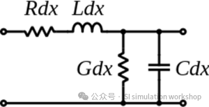
Now let’s break down these two types of losses and see how they affect overall loss.
Conductor Loss
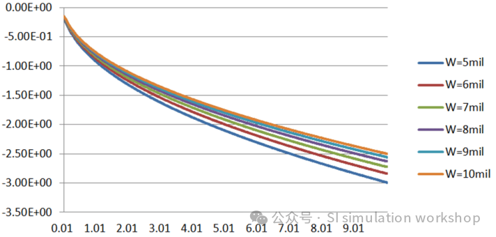
For conductor loss, the most intuitive factor is the resistance R of the conductor. We all know that the larger the cross-sectional area of the conductor, meaning the wider the trace or the thicker the material, the smaller the resistance will be, thus reducing the loss.
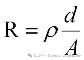
Conductor loss is proportional to the square of the frequency!
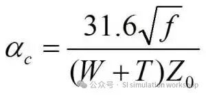
The impact of trace width on loss cannot be overlooked!
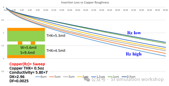
Another factor contributing to conductor loss is the roughness of the conductor.
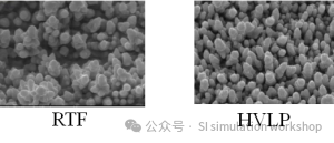
It is difficult to find a perfectly smooth surface in this world; while they may appear similar to the naked eye, a high-magnification microscope reveals tiny particles on the conductor’s surface, which vary in size depending on the type of copper foil. The larger the average particle size, the greater the loss, and vice versa.
In the image below, we can see two different types of copper foil, RTF (Reverse Treated Foil) and HVLP (Hyper Very Low Profile), where the difference in particle size is evident, with RTF being larger (Rz approximately 3um) and HVLP being smaller (approximately 1.5um-2um).
Currently, the best copper foil in traditional PCB manufacturing can reach an Rz of 0.9um, which significantly reduces loss compared to standard copper foil. However, the yield is still not excellent.
Dielectric Loss
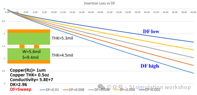
The primary cause of dielectric loss is the leakage current of the dielectric material and the rapid movement of molecules within the material when high-frequency signals change phase. This characteristic is typically described using the loss tangent factor, DF. The larger the DF value, the greater the dielectric loss. It can be observed that dielectric loss is almost proportional to frequency; the higher the frequency, the more severe the dielectric loss.

Additionally, it is worth mentioning that the voids in the glass fiber of the material can cause phase inconsistencies between the differential signals P/N, which can lead to resonance at high frequencies, worsening loss. Current solutions include rotating the board, using open weave fabrics (such as 1078/1035), Zig-Zag, Multi-ply, etc. However, this phenomenon may only become a major issue with the advent of PCIe Gen5 or 112G-PAM4.
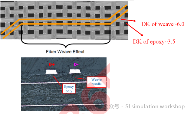
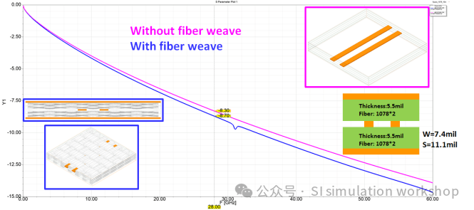
The last factor that can exacerbate loss is the Via stub.。
Via stubs occur because the signal routing does not completely transition from the top layer to the bottom layer, resulting in a small open stub in the plated through hole (PTH Via). This open stub can cause significant resonance in the routing, leading to increased loss!
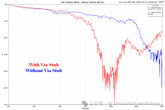
We have briefly listed several notable items regarding PCB losses for your reference.
【Do you often design PCBs? Scan the code to reply “PCB” and join our practical series group on the topic of “PCB Design”】