According to a report by Synergy Research Group, by the end of 2024, the number of data centers operated by hyperscale operators will reach 1,136, a significant increase from less than 600 in the fourth quarter of 2019, indicating that the number of global hyperscale data centers has nearly doubled in the past five years.Additionally, the number of planned data center projects in the coming years has increased by 60% since March 2022, rising from 314 to 504 by March 2025. These facilities are no longer single 10 megawatt (MW) data centers but rather large campuses covering hundreds of acres and exceeding 100 MW, consisting of multiple buildings.Earlier this year, SoftBank Group, OpenAI, and Oracle announced a $500 billion investment to create the “Interstellar Gateway” project to build infrastructure in the U.S. to support AI development.However, there are differing opinions in the market. “Large tech companies, investment funds, and other institutions are hastily building server bases from the U.S. to various parts of Asia, and this investment seems blind, with many server bases not clearly considering customer needs during construction,” said Alibaba Group Chairman Cai Chongxin at the HSBC Global Investment Summit on March 25. He warned that the current pace of global data center construction exceeds the initial demand for artificial intelligence (AI), raising concerns about a potential bubble risk.Moreover, Microsoft has canceled data center projects in Europe and the U.S. with a total power generation capacity of about 2 gigawatts, which may indicate that “the supply of data centers has exceeded current demand expectations.”Nevertheless, it is an undeniable fact that large-scale data centers have seen a geometric increase in energy consumption to support high-intensity AI computations in recent years. Some ultra-large data centers consume as much electricity annually as a small city. This not only leads to a significant increase in operating costs but also poses a severe challenge to global energy supply and sustainability.Power management, as a core technology for optimizing chip power consumption and improving energy utilization efficiency, along with the pursuit of high power density representing chip performance and space utilization, has become a research focus and competitive battleground in the AI chip field. Chip companies are also striving to enhance power density to meet the future demands of the AI industry.The following excerpts from white papers and insights published by several chip companies regarding AI servers all agree that silicon will not disappear in the future, while the demand for wide bandgap semiconductors will continue to grow.
ON Semiconductor: How SiC MOSFETs Improve Power Conversion Efficiency in AI Data Centers
Wonhwa Lee, product line manager at ON Semiconductor, stated that heat dissipation is a significant challenge faced by data centers. It is estimated that the power consumption of cooling systems in most data centers today accounts for over 40% of total power consumption. In fact, for power efficiency, wasted energy primarily dissipates in the form of heat, which must then be expelled by the data center’s air conditioning system. Therefore, the higher the power conversion efficiency, the less heat generated, and correspondingly, the lower the electricity costs for cooling.The power density within data centers is accelerating. About a decade ago, the average power density per rack was around 4 to 5 kW, but today, hyperscale cloud computing companies (such as Amazon, Microsoft, or Facebook) typically require a power density of 20 to 30 kW per rack. Some specialized systems even demand power densities exceeding 100 kW per rack. Due to limited space for power storage and heat dissipation, high power density requires compact and high-efficiency power designs, while also meeting specific industry requirements, such as AI data center PSUs needing to comply with strict Open Rack V3 (ORV3) basic specifications. Recently, new AC-DC PSUs have a nominal input range of 200 to 277VAC, outputting 50VDC, with ORV3 standards requiring peak efficiency exceeding 97.5% under 30% to 100% load conditions and a minimum efficiency of 94% under 10% to 30% load conditions.Power Factor Correction (PFC) stages are a critical component in the AC-DC conversion of PSUs and are essential for achieving high energy efficiency. The PFC stage shapes the input current to maximize the ratio of useful power to total input power. To meet electromagnetic compatibility (EMC) standards in regulations such as IEC 61000-3-2 and ensure compliance with energy efficiency specifications like ENERGY STAR®, PFC design is also crucial.For many applications, including data centers, it is best to use a “totem pole” PFC topology to design the PFC stage. This topology is typically used in the PFC function blocks of data center power supplies ranging from 3 kW to 8 kW systems (as shown below). The totem pole PFC stage is based on MOSFETs and improves the efficiency and power density of AC power supplies by eliminating bulky and lossy bridge rectifiers.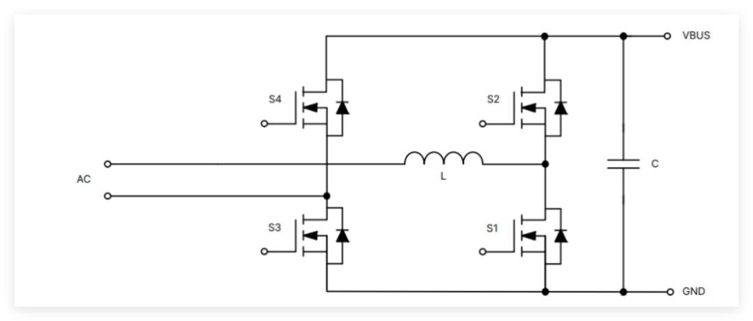 Figure: Totem Pole PFC StageHowever, to achieve the 97.5% or higher efficiency required by large-scale data center companies, the totem pole PFC must use MOSFETs based on “wide bandgap” semiconductor materials (such as silicon carbide (SiC)). Today, all PFC stages use SiC MOSFETs as fast-switching bridge arms and silicon-based super junction MOSFETs as phase or slow bridge arms.Compared to silicon MOSFETs, SiC MOSFETs offer superior performance, higher efficiency, and robust reliability, performing better at high temperatures and operating at higher switching frequencies.Compared to silicon-based super junction MOSFETs, SiC MOSFETs have lower energy stored in output capacitance (EOSS), which is crucial for achieving low load targets, as switching losses in the PFC stage primarily arise from EOSS and relatively high gate charge devices. Lower EOSS can significantly reduce energy loss during the switching process, thereby improving the efficiency of the totem pole PFC fast bridge arm. Additionally, due to the excellent thermal conductivity of SiC devices, which is three times that of silicon-based devices, SiC MOSFETs exhibit a better positive temperature coefficient RDS(ON) compared to silicon-based super junction MOSFETs.The following figure shows the relationship between the on-resistance of a 650V SiC MOSFET and junction temperature. (The on-resistance at a junction temperature of 175°C is 1.5 times higher than that at room temperature.)
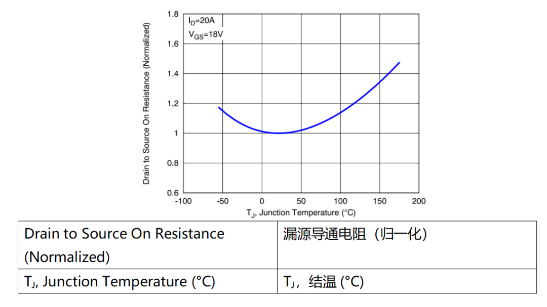
Figure: Relationship between On-Resistance of 650V SiC MOSFET and Junction TemperatureSimilarly, the following figure shows the relationship between the on-resistance of a 650V super junction MOSFET and junction temperature. The on-resistance at a junction temperature of 175°C is more than 2.5 times higher than that at room temperature.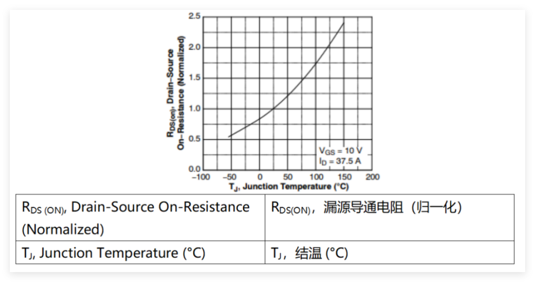 Figure: Relationship between On-Resistance of 650V Silicon-Based Super Junction MOSFET and Junction TemperatureComparing silicon-based 650V super junction MOSFETs with 650V SiC MOSFETs, at a junction temperature (Tj) of 175°C, the on-resistance RDS(ON) of the former increases to about 50 mohm, while the latter’s RDS(ON) is about 30 mohm. During high-temperature operation, the conduction losses of the 650V SiC MOSFET are lower.In the totem pole PFC slow bridge arm function block and LLC function block, conduction losses account for the majority of total power losses. The lower RDS(ON) of SiC MOSFETs at higher junction temperatures helps improve system efficiency.Thanks to the smaller increase in RDS(ON) at high temperatures and excellent EOSS, SiC MOSFETs perform outstandingly in totem pole PFC topologies, further enhancing efficiency and reducing energy loss.
STMicroelectronics: The Role of Hybrid TCM/CCM Control Strategies in Interleaved TTP PFC
STMicroelectronics states that AI servers, as key hardware supporting various complex AI computations, have their power supply (PSU) performance become a crucial factor determining the overall system performance. A significant innovation in the field of high-power AI server PSUs is the hybrid TCM/CCM control strategy, which plays an important role in interleaved TTP PFC.Advanced control strategies have become a necessary choice, such as TCM, CCM, and interleaved totem pole PFC technology, which can optimize power supply performance, allowing PSUs to respond quickly to load changes and achieve intelligent power management. Modular and scalable designs are also critical, meeting diverse power demands, facilitating maintenance and module replacement, and enhancing system reliability.Moreover, AI servers generate a lot of heat during operation, and efficient cooling and thermal management technologies are upgraded from air cooling to liquid cooling to ensure system stability. Enhancing fault tolerance and predictive maintenance capabilities, reducing downtime risks, and ensuring continuous power supply are important manifestations of high reliability in PSUs.Detailed Explanation of Hybrid TCM/CCM Control Strategy
-
Totem Pole PFC Topology
The totem pole PFC topology is widely used in PSU designs, mainly in single-channel and interleaved configurations. Single-channel totem pole PFC is typically suitable for power levels below 4kW, with fewer devices, a relatively simple circuit structure, and easy control implementation.
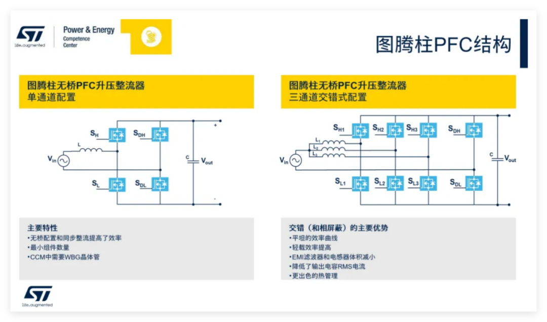
Interleaved totem pole PFC is suitable for high-power scenarios with higher power and efficiency requirements. It adopts two-phase or three-phase interleaving, allowing for more flexible operating modes, which can be CCM, TCM, or even hybrid modes. Under light load conditions, by adopting TCM mode and phase shielding technology, it can further enhance efficiency and reduce device losses, providing a more reliable solution for high-power AI server PSUs.
-
Comparison and Selection of Control Modes
In PFC control strategies, common modes include CCM (Continuous Conduction Mode), DCM (Discontinuous Conduction Mode), CRM (Critical Conduction Mode), and TCM (Triangle Current Mode). In this discussion, the focus is on the hybrid mode of CCM and TCM.CCM is characterized by continuous current and fixed switching frequency. This mode performs excellently in high power and high stability requirements because its current ripple is low, providing relatively stable current output, but its switching losses are higher, and efficiency may decrease under light loads.
TCM, on the other hand, is a control mode with variable switching frequency, where the current waveform is triangular. Its advantage lies in lower switching losses and higher efficiency under light loads. Compared to DCM and CRM, TCM and CCM are more suitable for AI server PSU applications. The discontinuous characteristics of DCM lead to unstable operating frequencies and cannot achieve zero-voltage switching, resulting in deficiencies in efficiency and stability. Although CRM is also a variable frequency mode, it similarly lacks the advantage of zero-voltage switching, so it has not been a focus in this application scenario. The combination of TCM and CCM can achieve zero-voltage switching, effectively improving overall efficiency and meeting the demands of AI servers under different load conditions.Advantages of Hybrid Control Modes
Hybrid TCM/CCM control modes have several significant advantages:Optimized Efficiency: The hybrid strategy can switch between TCM and CCM based on load conditions, optimizing efficiency across a wide range of operating points. TCM is more efficient under light loads due to reduced switching losses, while CCM is more efficient under high loads due to lower conduction losses.Reduced Ripple Current: Two-phase/three-phase interleaving helps significantly reduce input and output current ripple. The hybrid approach can further optimize ripple reduction by dynamically adjusting operating modes.Enhanced Thermal Management: Distributing the load between two phases and switching between TCM and CCM can lead to better thermal performance and more balanced heat distribution.Improved Transient Response: Switching between TCM and CCM allows the system to quickly adapt to load changes, providing better transient response.Flexibility and Reliability: The hybrid control strategy offers flexibility in design and application, making it suitable for various operating conditions. It can improve the reliability of PFC circuits by reducing stress on components and enhancing thermal management.Implementation of Hybrid Control Modes in Interleaved TTP PFC
-
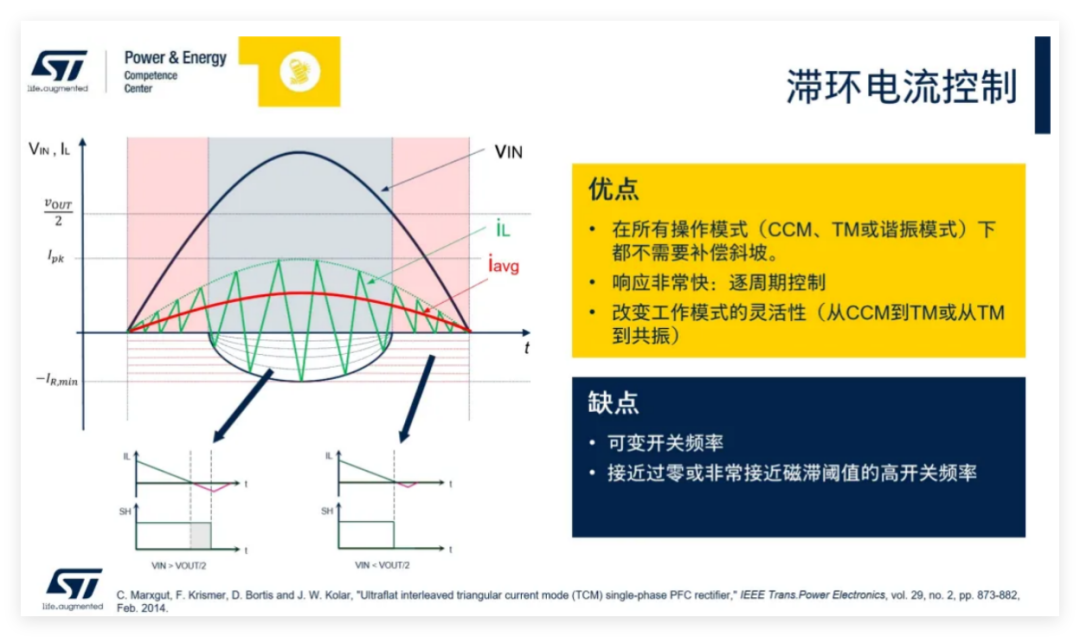
Hysteresis Current Control
In interleaved TTP PFC, one of the key technologies for implementing hybrid TCM/CCM control modes is hysteresis current control. By setting upper and lower limits for the inductor current, the inductor current fluctuates within this set range, achieving zero-voltage switching and effectively reducing switching losses. This control method responds quickly, allowing for precise control of current on a per-cycle basis, and the switching between operating modes is flexible, enabling rapid transitions between CCM, TCM, or other modes based on actual needs. However, it has high requirements for inductor current detection.
-
Current Detection Solutions
Due to the high requirements for inductor current detection in hysteresis current control, current sensors need to possess various characteristics. They must have isolation capabilities to ensure circuit safety; be capable of bidirectional detection since current can flow in both positive and negative directions; have low loss characteristics to minimize impact on system efficiency; achieve fast response and OCP protection to meet real-time control needs; and possess high bandwidth to accommodate variable frequency signals.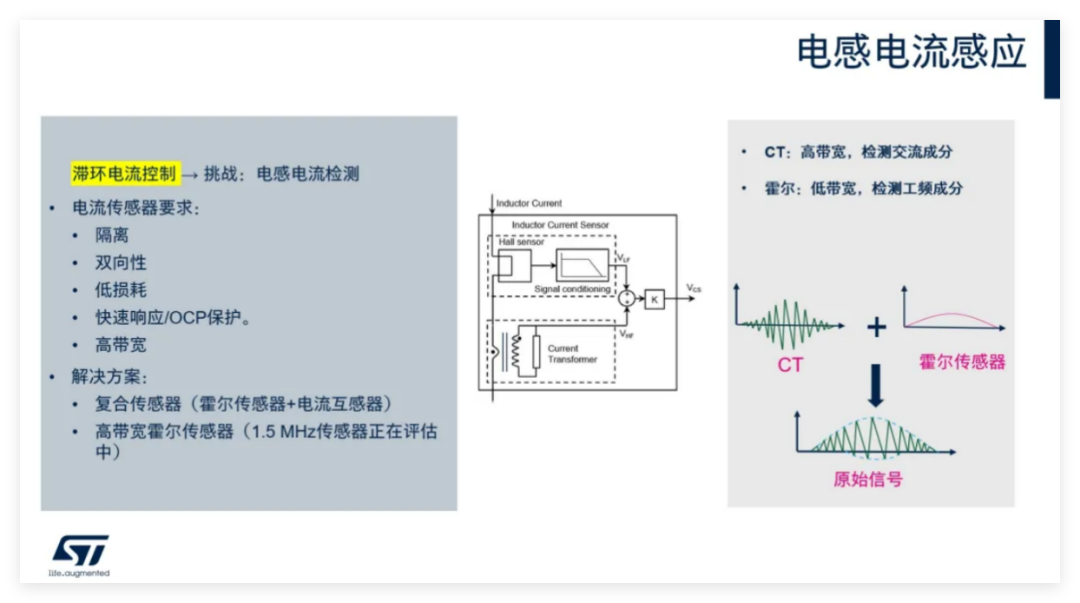 ST currently employs a composite solution that combines Hall sensors with current transformers (CT). The CT is primarily used to detect high-frequency components of AC, specifically the high-frequency electric noise in the inductor current; the Hall sensor is responsible for detecting the power frequency components. The signals collected by both are superimposed to obtain a raw signal that reflects the actual inductor current. Additionally, ST is evaluating high-bandwidth Hall sensors to explore better current detection solutions.At the hardware level, ST’s solution centers around the STM32G474 as the core control chip, paired with relevant power devices such as different types of MOSFETs to construct a complete control circuit. The STM32G474 has powerful processing capabilities and rich peripheral resources, providing a hardware foundation for implementing complex control algorithms.
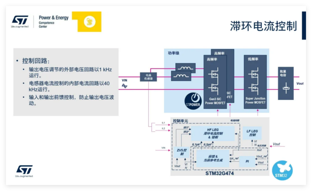
The solution utilizes the internal DAC, fast comparators, and high-resolution timers (HRTIM) of the STM32G474 to achieve hysteresis control, ZVS (zero-voltage switching) control, and drive signal output. The control loop includes a voltage outer loop running at 1kHz, primarily aimed at stabilizing the output voltage to maintain it at the set value; and a current inner loop running at 40kHz for precise control of inductor current. Additionally, input and output feedforward control is introduced to effectively prevent output voltage fluctuations and improve system stability.
CCM Implementation and Simulation Test Results
There are two common implementation methods for entering CCM mode: fixed ripple band and fixed switching frequency. Taking fixed ripple band as an example, if the ripple band is set to 4A, the entire control process operates in variable frequency. The other method is fixed switching frequency, for example, set at 70kHz, in which case the inductor ripple must be calculated based on input voltage (Vin), output voltage (Vout), period (T), and inductance (L). Through simulation, current waveforms under different methods have been obtained. Currently, the fixed ripple band method is used in practical applications.
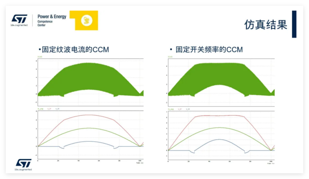
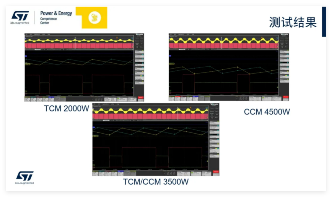
From the test results, under different load conditions of 2000W (pure TCM), 3500W (TCM/CCM hybrid), and 4500W (CCM dominant), the current waveforms performed well. For instance, in the 2000W pure TCM mode, the current waveform interleaved well; in the 3500W hybrid mode, the transition area between CCM and TCM was smooth; and in the 4500W mode, where CCM was dominant, the CCM interval operated stably. These results fully validate the feasibility and effectiveness of the solution, especially as the zero-crossing portion of the current showed no significant distortion, demonstrating ideal performance and significantly enhancing PFC performance, providing reliable assurance for the practical application of AI server PSUs.
Thus, the application of hybrid TCM/CCM control strategies in interleaved TTP PFC has brought significant performance improvements to high-power AI server PSUs. ST has meticulously crafted a professional design kit for high-power AI server power supplies and offers a comprehensive product portfolio to fully meet diverse design needs, injecting strong momentum into the development of AI server power supplies. Looking ahead, this technical system is expected to continue optimizing, laying a solid power foundation for the development of the AI field.
Infineon: The Need for Hybrid Power Semiconductors in PSU Architecture
Infineon states that future PSUs will require a combination of silicon-based, silicon carbide, and gallium nitride solutions to fully leverage the advantages of devices in different scenarios.Limitations of Silicon-Based Devices: Silicon has long dominated the power electronics field, but it faces physical limitations in handling high voltage, current, and frequency, nearing theoretical limits, making it difficult to further enhance efficiency and power density.Advantages of Wide Bandgap Devices: SiC and gallium nitride (GaN) exhibit higher figures of merit (FoM), performing better in efficiency and power density. Compared to silicon transistors, GaN transistors have lower output charge, no body diode recovery issues, low reverse recovery charge, low gate charge, and low temperature coefficient; SiC MOSFETs have low reverse recovery charge, minimal variation in on-resistance with temperature, low output charge, and more linear characteristics, along with low gate charge.Benefits of Hybrid Technology: Combining SiC and GaN technologies with existing silicon-based designs can bring significant advantages in efficiency, power density, and overall performance.
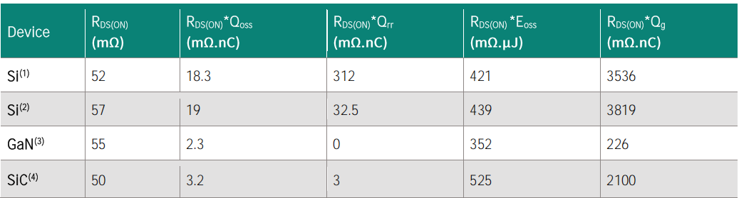
Figure: Comparison of FOM for Various ProductsInfineon’s innovative PSU solutions optimize each stage through a hybrid component approach that combines Si, SiC, and GaN technologies, achieving high power density and efficiency while reducing energy losses and improving thermal performance.These PSU solutions are rated from 3kW to 12kW, with benchmark efficiencies of 97.5%, suitable for the next generation of AI data centers, helping to reduce the carbon footprint of data centers.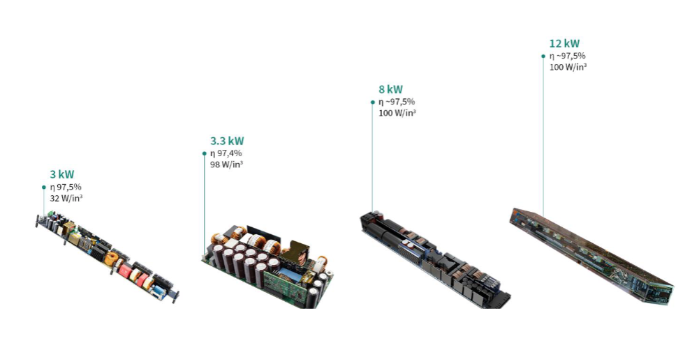 For example, Infineon’s 8kW PSU reference design:
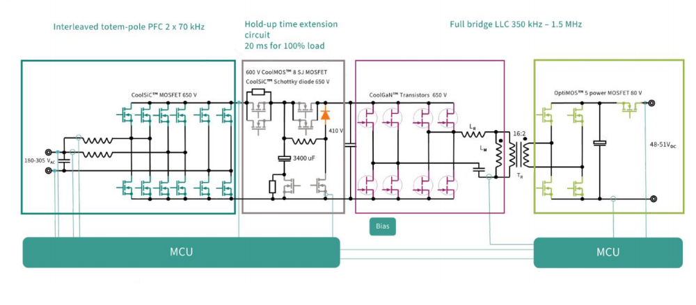 Bridge-Less Totem Pole PFC Stage: This reference board’s bridge-less totem pole PFC stage uses silicon carbide, helping to improve efficiency and reliability. The bridge-less totem pole PFC topology can reduce power losses from bridge rectifiers in traditional PFC topologies, thereby enhancing overall efficiency. For instance, when meeting the 80 Plus Titanium certification (which requires end-to-end peak efficiency exceeding 96%, meaning PFC stage efficiency must exceed 98.6%), traditional PFC topologies struggle to meet this standard due to power losses from bridge rectifiers, while the bridge-less totem pole PFC topology requires only one PFC inductor and can perform boost operations throughout the entire AC cycle, achieving high power density and high efficiency in PSU design.High-Frequency LLC Stage: The high-frequency LLC stage employs CoolGaN switches, whose lower capacitance characteristics enable faster switching, reducing energy losses during the switching process. This advantage of GaN transistors is particularly evident in high-frequency applications, helping to improve the power density and overall efficiency of power supplies. In some high-frequency power conversion circuits, GaN transistors can achieve faster switching actions, reducing switching losses and thus enhancing the performance of the entire power supply system.Application of Silicon Power Switches: Silicon power switches are used in the rectification stages of PFC and DC-DC phases because switching losses are minimal in these stages, and silicon power switches have extremely low on-resistance, allowing for effective utilization of this characteristic to minimize conduction losses and further enhance power supply efficiency. In actual power supply designs, by carefully selecting silicon power switches, energy losses during the rectification process can be effectively reduced, improving the overall performance of the power supply.High Efficiency: Achieving a benchmark efficiency of 97.5%. Optimized Low Cooling Requirements: Design optimizations have reduced cooling workload.High Power Density: Power density reaches 100W/in³, which is twice the ORv3 specification. High power density allows PSUs to provide greater power output within limited space.
Nexperia: Mixing Silicon Carbide and Gallium Nitride
Nexperia also states that silicon-based power supplies have many limitations. For example, in a 12V, 1.5kW CRPS, LLC topology design must balance transformer winding, synchronous rectifier switching and conduction, power supply terminals, and other losses. Increasing switching frequency can reduce the size of magnetic components but will increase terminal losses; using multiple transformers can avoid terminal losses but will increase size.Frequency Limitations: The typical switching frequency of CRPS LLC converters on the market is 100 – 150kHz, while a 1.5kW server PSU may reach a switching frequency of 600kHz, exceeding the practical limits of silicon power MOSFETs, necessitating the use of gallium nitride high electron mobility transistors as synchronous rectifiers to meet 80 PLUS Titanium efficiency requirements.Application and Challenges of GaN Technology: GaN transistors perform excellently at high switching frequencies. Based on this, Nexperia has designed multi-kilowatt CRPS reference solutions, such as a 4.5kW design with a single 54V output and a switching frequency of 300kHz, meeting CRPS 185mm size requirements. However, gallium nitride also faces some challenges, such as the gate voltage range of GaN MOSFETs being -10V to 7V, with a threshold voltage of 1V to 2V, making them more fragile compared to silicon MOSFETs. Abnormal situations such as voltage spikes and ringing can easily damage their gates, as negative spikes in gate-source voltage (VGS) can occur when the low-side transistor turns off, and the gate loop inductance and high di/dt can cause VGS ringing, along with the risk of shoot-through current.
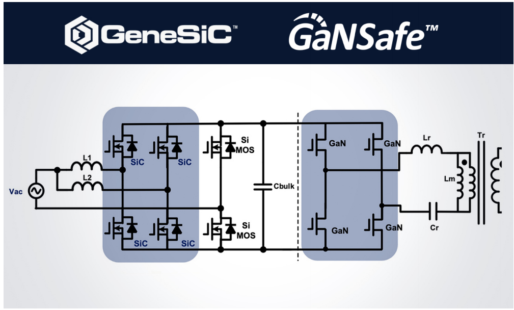 Nexperia’s solution is to integrate an optimized gate driver with GaN HEMTs in the same package, controlling the inductance and resistance values between the driver and the gate, reducing gate loop inductance to prevent excessive peak voltages; utilizing integrated protection features within the package simplifies power supply design.Combining GeneSiC MOSFETs enables efficient operation of bridge-less totem pole power factor correction (PFC) in continuous conduction mode, creating a 4.5kW CRPS185 module with a power density of 137W/in³, far exceeding silicon-based technology.Additionally, Nexperia has recently announced a strategic partnership with GigaDevice, aiming to integrate GigaDevice’s advanced high-performance MCU products with Nexperia’s high-frequency, high-speed, and highly integrated gallium nitride technology to create intelligent, efficient, and high power density digital power products. This collaboration will leverage GigaDevice’s comprehensive management capabilities across the entire industry chain and Nexperia’s deep understanding of system applications to accelerate commercialization in AI data centers, photovoltaic inverters, energy storage, charging piles, and electric vehicles. As part of this strategic partnership, GigaDevice will also work with Nexperia to establish a joint R&D laboratory, merging both parties’ technical expertise and ecological resource advantages to drive innovation and upgrades in intelligent and efficient power management solutions.
Texas Instruments: GaN Can Do It All
GaN enables high-frequency switching, which can reduce the size of passive components, thereby increasing density. Compared to silicon and silicon carbide, GaN also reduces switching, gate drive, and reverse recovery losses, thereby improving power supply design efficiency. A 650V GaN FET can be used for AC/DC to DC/DC conversion, and 100V or 200V GaN FETs can be used for DC/DC conversion to achieve power supply.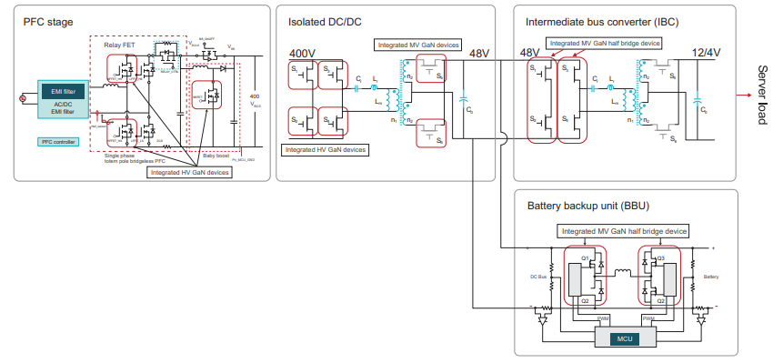 For 650V power supplies, Texas Instruments integrates 650V TOLL gallium nitride, which can convert AC power sources into DC buses through PFC and DC/DC stages. Texas Instruments’ GaN devices in TOLL packages can achieve over 99% efficiency at the PFC stage and over 98% efficiency at the DC/DC stage.For 100V to 200V GaN, there are three possible systems:Power Supply Unit (PSU): Changes in the open compute project are increasing the popularity of 48V outputs; however, the losses (gate drive and overlap losses) of the required 80V and 100V silicon solutions have significantly increased compared to previous solutions. GaN solutions such as LMG3100 help minimize the aforementioned losses in the secondary synchronous rectifier of the inductive-capacitive-capacitor (LLC) stage.Intermediate Bus Converter (IBC): This system converts the intermediate voltage (48V) output from the PSU to a lower voltage, which is then delivered to the server. With the popularity of the 48V voltage level, IBC helps reduce I²R losses in server subsystems and decreases the size and cost of busbars and power transmission lines. The downside of IBC is that it adds an additional step in power conversion, which may impact efficiency. Therefore, in addition to several new topologies that OEMs have tested to achieve the best combination of high efficiency and high power density, it is essential to fully utilize efficient GaN devices such as LMG2100 and LMG3100.Battery Backup Unit: Buck/boost stages typically convert battery voltage (48V) to bus voltage (48V). When the mains power line is down and power flow is bidirectional, you can also use the BBU for battery power conversion. Uninterruptible power supplies use this stage because it performs a single DC/DC conversion directly through the battery, avoiding losses caused by AC/DC/DC conversions.
Innoscience – Recent Collaboration with Great Wall Power
Recently, Great Wall Power announced that it has adopted Innoscience’s gallium nitride (InnoGaN) technology in its titanium-grade power supplies for AI data centers, achieving ultra-high power conversion efficiency exceeding 96%, surpassing the highest global 80PLUS Titanium efficiency standard.To address the energy consumption dilemma of server power supplies, Innoscience has pioneered the introduction of E-GaN power ICs (ISG612xTD SolidGaN) in a To-247-4 package, integrating gate drivers and short-circuit protection, with a voltage rating of 700V and Rdson ranging from 22 to 59mΩ. This series of products integrates precision Vgs gate drivers, featuring fast short-circuit protection and excellent thermal performance, capable of meeting the high-frequency switching required for Titanium Plus efficiency, achieving more than double the power density compared to traditional solutions.The OCTC “High Power Density Server Power Modular Design White Paper (2024)” shows that during 80% of server operating time, in the typical load range of 20%-50%, the power conversion efficiency of gallium nitride titanium power supplies can stabilize above 95.5%-96%, effectively avoiding hidden energy consumption caused by “efficiency gaps.” Great Wall server power supplies are the first to adopt Innoscience’s co-packaged chips ISG6122TD and ISG6123TD, reducing energy losses by at least 30% in light to medium loads compared to traditional power supplies, achieving a 4 percentage point improvement in the 20%-50% typical load range, and realizing over 96% conversion efficiency. It is estimated that adopting gallium nitride titanium power supply solutions can save over 2 million yuan in electricity costs per year for every 10,000 servers, reduce heat generation by 50%, and drive down air conditioning energy consumption by 18%. This significantly promotes the PUE of intelligent computing centers to break below 1.2, achieving dual benefits of “energy saving + heat dissipation.”
Conclusion
Whether it is gallium nitride or silicon carbide, both have gradually matured in the AI server field and will increasingly gain market favor, especially as demands for power density, efficiency, size, conversion frequency, and other factors continue to grow, this market will remain hot in the future.
· END ·
Follow the subscription account of EEWorld: "Robot Development Circle"
Reply "DS" to receive the complete version of "DeepSeek: From Beginner to Pro"

Scan to add the assistant and reply “Robot”
Join the group to exchange experiences face-to-face with electronic engineers