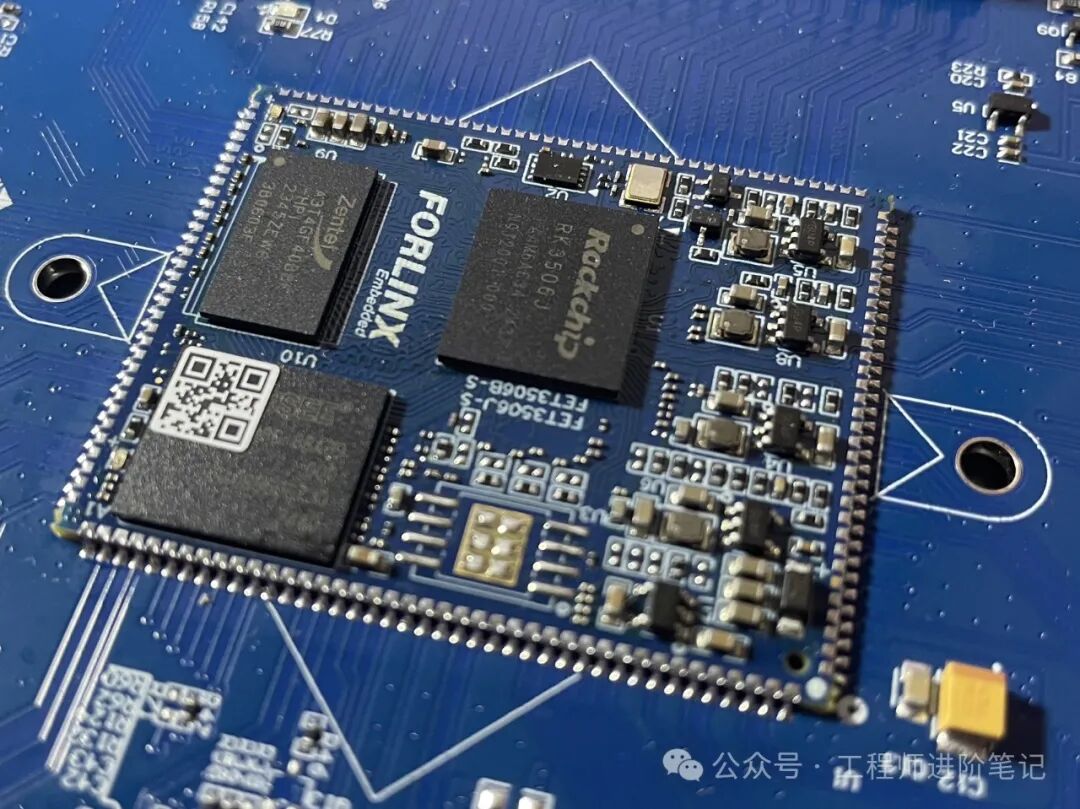
I am Lao Wen, an embedded engineer who loves learning.Follow me to become even better together!As an amateur embedded engineer, my main job involves using microcontrollers to detect button actions and implement various LED light effects (advanced lighting). Occasionally, I also design simple circuit boards and solder some smart hardware to validate ideas or technical solutions.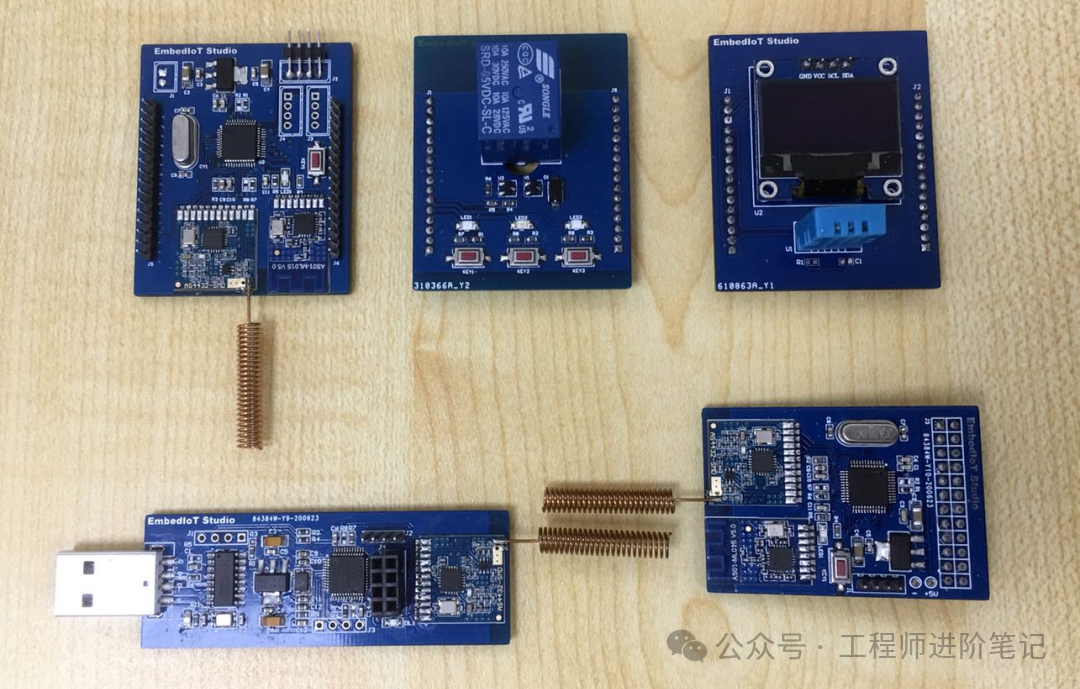 During my free time, I enjoy tinkering with embedded Linux development boards, as I believe my technical skills should not remain limited to buttons and lights; I need to explore more advanced technologies.I have already tested several embedded Linux development boards and have gained considerable insights into setting up development environments. You can click the link below for a recap.Embedded software and hardware development relies heavily on excellent documentation!Does setting up an embedded AI development environment discourage many beginners?Apple’s iPhone 16 has been released; how high is the degree of localization for embedded HarmonyOS?High-performance Linux development boards typically adopt a design approach of 【core board + base board】. Initially, I was curious why the CPU isn’t designed on the same circuit board.After some research, I found that this separation design is based on practical application considerations by the development board manufacturers. The core board usually contains the 【CPU + memory + storage + power management】 chips, which are all critical components with high bandwidth and communication rates.The base board typically includes peripheral devices and communication interfaces, which do not impose as high requirements on the number of layers and specifications of the circuit board. Separating the core board allows for a balance between cost and stability.(Artistic embedded Linux core boards)
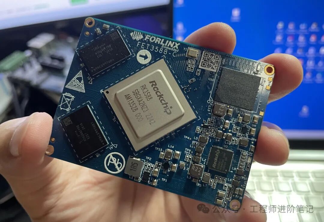
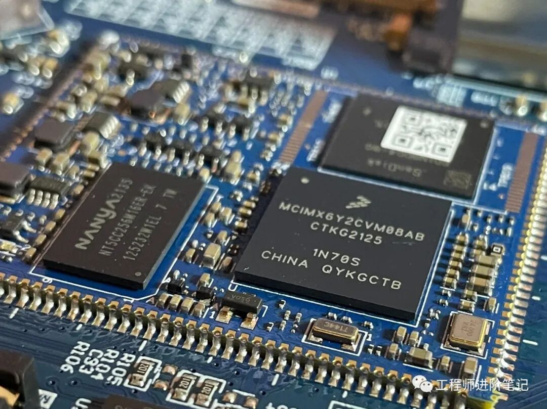 Seeing these artistic core boards, I once thought that if I could design a core board and then use it with different functional base boards, it would be a very fulfilling achievement.However, reality is often harsher than ideals. After learning about the design details of these embedded Linux core boards, I realized it is not as simple as I imagined!These embedded Linux core boards with more than six layers require attention to numerous factors during the design process, such as: stacking structure, component layout, power layout, power and ground routing, high-speed signal routing, impedance control, electromagnetic interference control, manufacturability design, test point setup, etc.Let’s first understand what a high-layer PCB is.In simple terms, it is a circuit board designed with circuit traces on each layer, which are then stacked and bonded together using insulating materials and lamination processes. The interconnections between different circuit boards are made using vias, as shown in the image below, truly high-layer PCB~
 When space is limited, the more layers a circuit board has, the more freedom a PCB layout engineer has to work with, allowing for higher circuit density and more complex circuit designs.High-layer PCBs can provide better electromagnetic compatibility and signal integrity for hardware products, but they also make PCB design and manufacturing more complex and expensive.With so many circuit layers, how can they be laminated so thinly during production while ensuring that they are insulated from each other and do not short-circuit? What is the production process for high-layer PCBs?
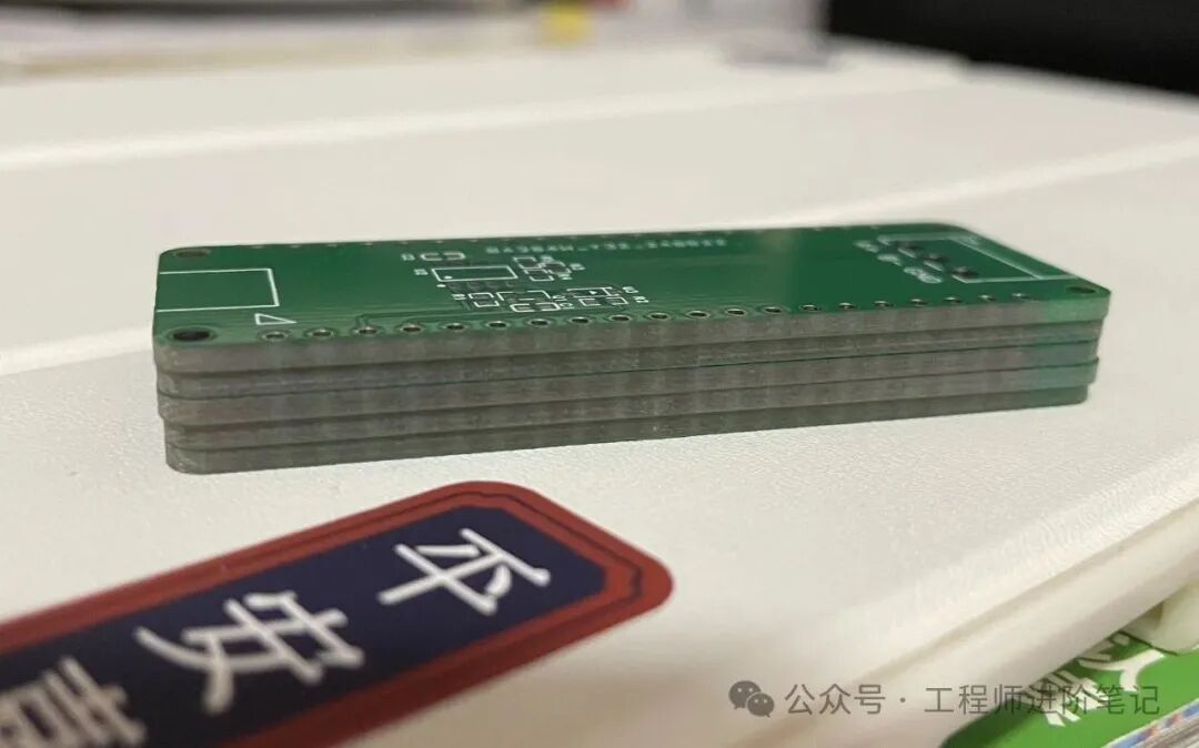
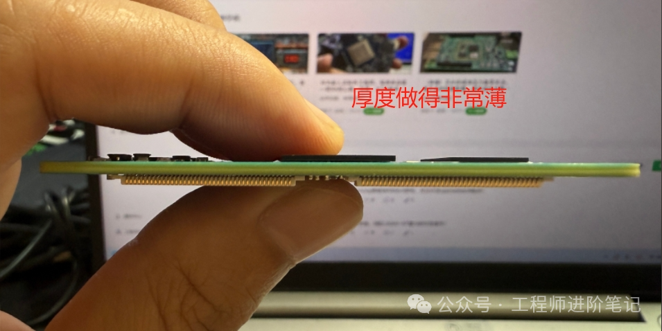 The thickness of a 10-layer circuit board is 1.6 mm.Before a PCB factory starts manufacturing PCBs, the layout engineer usually needs to perform some preliminary work, including submitting and reviewing manufacturing information (Gerber files, drilling files, netlist data), as well as selecting circuit board materials.In the production of high-layer boards, if we were to detail the entire process, it would typically involve over 200 different processing steps. (It would take a whole day to explain!)(—— Knowledge Sharing START ——)Let’s take the lamination process of circuit boards as an example! For instance, by combining different specifications of prepreg and copper-clad laminates, various thicknesses of circuit boards can be achieved. The manufacturing method of a rigid 6-layer PCB and the elements between each layer are shown in the image below.
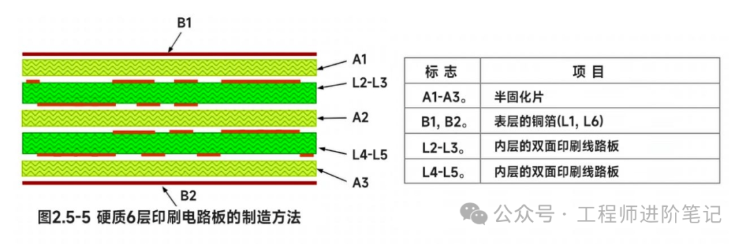 By carefully observing the layers in the image, you can see that they are all symmetrical and have the same thickness, such as: A1, A2, and A3, B1 and B2, L2-L3 and L4-L5. The inner copper foils are also evenly distributed to avoid distortion of the circuit board caused by uneven thermal stress.Whether these multiple layers can be accurately laminated together is crucial for the quality of high-layer circuit boards! If there is a slight misalignment between certain layers, it could lead to open or short circuit issues.Therefore, before the lamination process, an AOI (Automated Optical Inspection) is usually performed to visually compare the actual copper circuit with the design files. If defects are found at this stage, they can still be repaired.(Once laminated, repairs are either impossible or very costly)Once everything is confirmed, the layers can be laminated together. The A1, A2, and A3 in the image are used for insulation. These insulating materials (epoxy resin) will melt when heated and bond the copper-clad layers together, acting like glue. The layers are electrically connected through metallized vias.Why is the precision of this lamination process so important? This is because the insulating material will flow between each board layer when melted, and any variation in thickness will affect the distance between the layers, which has the greatest impact on the characteristic impedance of controlled impedance transmission lines.
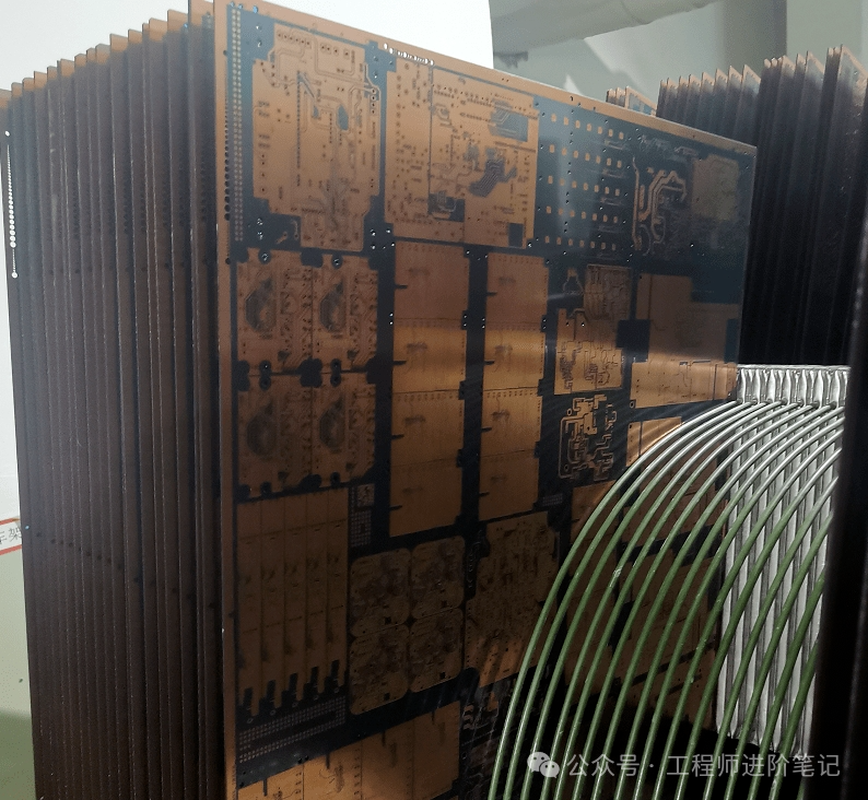 The spliced production of circuit boardsThe final production design of high-layer PCBs involves splicing multiple small-area boards onto a large-area substrate for production (commonly known as panelization). The uniformity of the flow of insulating materials during lamination of such a large substrate is critical, and the lamination equipment plays a crucial role.
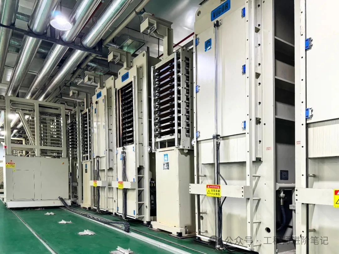 The Taiwan Vigor fully automatic laminating machineThe lamination process of a circuit board involves so many knowledge points and considerations to learn! It’s incredibly complex!(—— Knowledge Sharing END ——)Returning to the design phase of multilayer circuit boards, layout engineers(PCB Layout Engineers)can directly enhance the quality of multilayer circuit boards by selecting certain specified manufacturing processes during the design phase.For example, embedded Linux core boards with more than six layers typically specify the use of gold immersion process! The so-called gold immersion process involves depositing a layer of nickel-phosphorus alloy on the surface of the PCB pads, followed by a layer of gold. This process can improve the corrosion resistance, conductivity, and solderability of the circuit board, making it look very attractive with its golden sheen, which everyone loves!(Theoretically, the thicker the gold immersion, the more expensive it is!)(In fact, the production cost of the gold immersion process is also decreasing. At Jialichuang, for PCBs with 6-32 layers, gold immersion is free and can be thickened to 2u”.)
 Golden padsIn addition to using the gold immersion process, layout engineers can also use via-in-pad techniques, especially when designing multilayer circuit boards. By placing vias directly in the chip pads, the workload of the layout engineer can be significantly reduced, greatly facilitating routing.In general, if via-in-pad is not used and regular vias are employed, the vias may gradually corrode during use, leading to circuit connection failures, signal degradation, open circuits, or short circuits, all of which can affect product reliability.
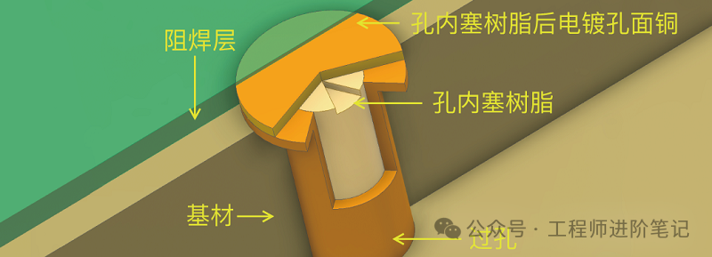 Via-in-pad schematicDue to the complexity of the manufacturing process, many PCB factories charge for via-in-pad, but at Jialichuang, via-in-pad has long been available for free.In addition to gold immersion and via-in-pad, the quality of circuit boards can also be improved by using positive photoresist process instead of negative photoresist process. You can find more information about these two processes online, so I won’t elaborate further here.The knowledge points regarding multilayer circuit board design mentioned above are just a tiny fraction of the entire design and manufacturing process. In reality, if we were to detail all the design and manufacturing intricacies of the entire PCB industry chain, it could fill a book.For books on circuit board design and manufacturing, I recommend the following: “From Design to Mass Production: A Practical Guide for Electronic Engineers on PCB Manufacturing”, which may interest hardware circuit board engineers.Jialichuang has launched a new PCB book: 500,000 words of practical knowledge to avoid pitfalls from design to production.
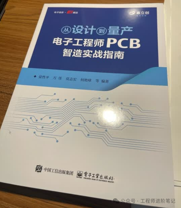 Some materials sourced from: Jialichuang, the internet.
-END-
Previous Recommendations: Click the image to jump to read
What skills should embedded software engineers develop besides coding?
Embedded software engineers, shattered by late-night hardware debugging.
Embedded software and hardware are at odds, and the project is stalled!
I am Lao Wen, an embedded engineer who loves learning.Follow me to become even better together!