In the previous article of this packaging series, I introduced the chip-on-board process. Here, I will provide a brief overview of another “unassuming” process in semiconductor packaging—Underfill.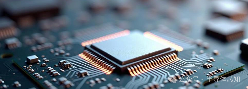 In the semiconductor packaging system, Underfill is a very inconspicuous yet crucial process (in fact, every process is important…). Whether it is Flip-Chip, 2.5D CoWoS, or the latest 3D hybrid bonding structure, as packaging trends towards high density, small pitch, and large area, the mechanical stress between the chip and substrate rapidly amplifies. Traditional solder joints can no longer bear the fatigue damage caused by thermal cycling alone, and Underfill has been pushed to the forefront in this context. It may seem like just a layer of “injected adhesive,” but it determines the lifespan, reliability, and long-term yield of chip packaging, making it one of the most critical material processes for optimizing packaging reliability.(1) What is Underfill?If we consider Flip-Chip as placing the chip “upside down” on the substrate, then the solder joints are the only bridge for all electrical and mechanical connections. However, as the coefficient of thermal expansion (CTE) mismatch between silicon and the substrate continues to widen, every power change that causes a temperature rise puts the solder joints under micro-level stretching. After over 2000 power cycles, this accumulated stress is enough to cause fatigue cracks in the solder joints. Underfill is a low-modulus, high-flow resin material that fills around the solder joints, forming a “whole” between the chip, solder joints, and substrate, dispersing thermal stress from the solder joints to a larger volume. This mechanism gives the solder joints, which originally bore the stress alone, a “mechanical exoskeleton.” In today’s advanced packaging, which is moving towards larger chips, multi-chip configurations, and high power, the thermal cycling lifespan improvement brought by Underfill is an indispensable foundational support in the competition for yield and cost.(2) Introduction to Underfill ProcessThe traditional Underfill process mainly relies on capillary flow (Capillary Underfill, CUF), where resin is injected from the side after the chip has been soldered, allowing it to flow spontaneously to the bottom of the chip. However, as the solder joint pitch decreases from 150 μm to 40 μm, and then to 20 μm, the speed, uniformity, and dead zone issues of this method gradually become bottlenecks.As a result, the packaging industry has begun to shift towards pre-applied processes (Pre-Applied Underfill), with the most typical being NCF (Non-Conductive Film), where Underfill is applied in a thin film form on the wafer or substrate before the chip is attached, allowing the chip + Underfill flow + curing to be completed simultaneously, improving efficiency and reducing residual voids.Moving into the 2.5D/3D era, different forms of Underfill materials have been further introduced, such as Micro-UF for filling TSV areas, ultra-low modulus UF for Hybrid Bonding, and Mold-UF for large area reinforcement in Chiplet packaging. Underfill is no longer just about “injecting adhesive”; it has become a material system that evolves with packaging structures, requiring a new UF formulation and process window for each generation of packaging structure.(3) Is Underfill one of the focal points of advanced packaging competition?The greatest value brought by Underfill is reliability, but during mass production, it is also one of the most challenging aspects to optimize in the entire packaging line. First, there is the balance between curing time and capacity; CUF curing often takes tens of minutes to several hours, which is a typical bottleneck in Flip-Chip production lines. Secondly, there are issues with voids and insufficient adhesive; any tiny bubble can become a source of cracks during thermal cycling. More importantly, in 2.5D and 3D packaging, Underfill not only affects mechanical strength but also directly impacts heat dissipation paths, warpage control, SMT reflow reliability, and even electrical performance. Due to this series of complexities, material manufacturers (such as Namics, Henkel, Shin-Etsu, and Sumitomo Chemical) are launching specialized Underfill systems for different structures, while wafer fabs are continuously optimizing process windows to improve filling uniformity and reduce curing stress.With the ongoing development of Hybrid Bonding, Chiplet, small-pitch RDL, and high-power AI chips, Underfill will transition from a “reliability auxiliary material” to a leading role in advanced packaging design, becoming a core technology module that determines packaging feasibility, lifespan, and cost.