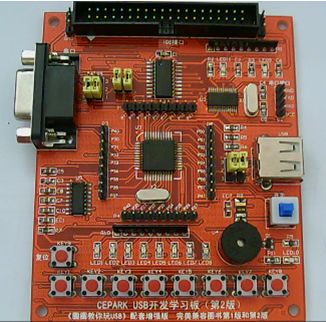
1) STC89C52
The STC89C52 microcontroller is a model from the STC89 series of microcontrollers. The STC89 series microcontrollers are a new generation of high-speed/low-power/highly anti-interference microcontrollers launched by Holtek Technology. The instruction code is fully compatible with traditional 8051 microcontrollers, and 12 clock/machine cycles and 6 clock/machine cycles can be selected arbitrarily. The HD version and 90C version integrate the MAX810 dedicated reset circuit internally.
2) USBD12
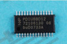
The PDIUSBD12 is a performance-optimized USB device, typically used in microcontroller-based systems and communicates with the microcontroller via a high-speed general-purpose parallel interface, also supporting local DMA transfers.
This device implements a USB interface in a modular way, allowing the selection of the most suitable microcontroller from many available options, enabling the use of existing architectures and minimizing firmware investment. This flexibility reduces development time, risk, and cost, providing the fastest route to developing low-cost and efficient USB peripheral device solutions.
The PDIUSBD12 is fully compliant with the USB 1.1 specification. It can also adapt to the design of most device class specifications, such as imaging, mass storage, communication, printing, and human input devices. Therefore, the PDIUSBD12 is very suitable for many peripheral devices, such as printers, scanners, external mass storage devices, Zip drives, and digital cameras. Many devices currently implemented with SCSI can directly reduce costs if implemented with USB. The low power consumption of the PDIUSBD12 when suspended and the LazyClock output meet the requirements of ACPI OnNOW and USB power management devices. Low power operation allows for bus-powered peripheral devices. The PDIUSBD12 also integrates features like SoftConnect, GoodLink, programmable clock output, low-frequency crystal oscillators, and termination resistors. All these features can save costs during system implementation while making it easy to achieve more advanced USB functionalities on peripheral devices.
3) MAX232
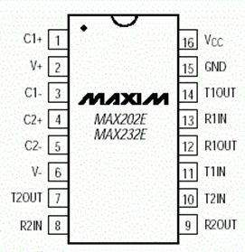
The MAX232 chip is a single-supply level-shifting chip designed by Maxim Integrated specifically for the RS-232 standard serial port of computers, powered by a +5V single supply.
Pin Description
The first part is the charge pump circuit, consisting of pins 1, 2, 3, 4, 5, 6 and 4 capacitors. Its function is to generate +12V and -12V power supplies to meet the needs of RS-232 serial port levels.
The second part is the data conversion channel, consisting of pins 7, 8, 9, 10, 11, 12, 13, and 14 forming two data channels.
Among them, pin 13 (R1IN), pin 12 (R1OUT), pin 11 (T1IN), and pin 14 (T1OUT) make up the first data channel.
Pin 8 (R2IN), pin 9 (R2OUT), pin 10 (T2IN), and pin 7 (T2OUT) make up the second data channel.
TTL/CMOS data is converted from T1IN and T2IN to RS-232 data output from T1OUT and T2OUT to the computer’s DB9 connector; RS-232 data from the DB9 connector is input from R1IN and R2IN and converted to TTL/CMOS data output from R1OUT and R2OUT.
The third part is the power supply, with pin 15 as GND and pin 16 as VCC (+5V).
Main Features
1) Complies with all RS-232C technical standards
2) Requires only a single +5V power supply
3) On-chip charge pump with boost and voltage polarity reversal capabilities, able to generate +10V and -10V voltages V+ and V-
4) Low power consumption, with a typical supply current of 5mA
5) Internally integrates 2 RS-232C drivers
6) Internally integrates 2 RS-232C receivers