The PMU (Power Management Unit) is responsible for supplying power to the SoC (System on Chip), regulating voltage and current to ensure the normal operation of various modules. Power integrity is crucial for ensuring that the Power Distribution Network (PDN) can provide stable and clean voltage and current, avoiding noise interference with the normal operation of the SoC.
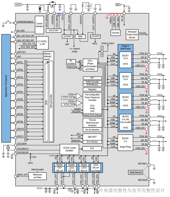
So, what exactly does power noise refer to? It may include voltage fluctuations, high-frequency noise, ground bounce, etc. These noise sources can originate from the PMU’s own switching noise, such as the switching operations of DC-DC converters, or from other external factors like load transient changes and PCB layout issues.
Next, we need to consider how the PMU’s power noise is transmitted to the SoC. The PMU typically powers the SoC through power rails, and if the voltage output from the PMU has noise, this noise will propagate through the power network to various parts of the SoC. The SoC may have multiple power domains, and different modules have varying sensitivities to power noise. For example, digital circuits may tolerate some high-frequency noise, but analog circuits such as ADCs and PLLs are very sensitive to noise and can easily be disturbed.
If power integrity is compromised, it may lead to various issues in the SoC, such as timing errors, degraded signal integrity, increased bit error rates, and even system crashes. Therefore, noise control in the PMU is crucial for the stable operation of the SoC.
Next, we will analyze the specific mechanisms of the impact. For instance, whether the PMU’s switching frequency overlaps with the sensitive frequency bands of the SoC. If the frequency of the PMU’s switching noise is close to the operating frequency of certain circuits within the SoC, it may cause resonance, amplifying the noise impact. Additionally, the impedance characteristics of the power distribution network are also important; if the PDN has high impedance at high frequencies, the noise voltage will be larger, leading to unstable power supply voltage for the SoC.
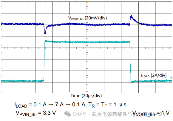
We also need to consider the PMU’s load transient response. When the SoC’s load suddenly changes, such as switching from low power mode to high performance mode, the PMU needs to quickly adjust the output voltage to maintain stability. If the PMU’s response speed is not fast enough, or if overshoot or undershoot occurs during the transient response, this will cause voltage fluctuations, affecting the power integrity of the SoC.
Moreover, PCB layout and packaging design can also affect noise transmission. For example, whether the power path between the PMU and the SoC is short enough, whether there are sufficient decoupling capacitors, and whether the ground plane design is good can all impact noise propagation and suppression.
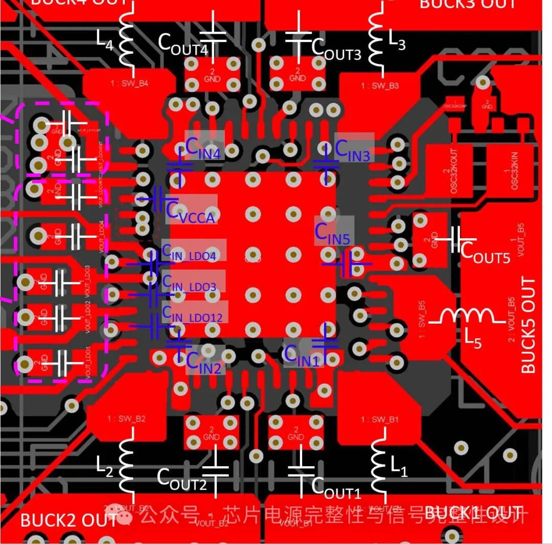
Possible solutions include optimizing the PMU design, such as using more efficient DC-DC converter topologies, increasing filter capacitance, and improving feedback control loops to enhance transient response. Additionally, on the SoC side, it may be necessary to design a more robust power distribution network, properly arrange decoupling capacitors, use power isolation techniques, and conduct thorough power integrity simulations and tests.
Attention should also be paid to some chip details, such as whether the sensitivity of the SoC to power noise varies across different process nodes, or the collaborative design strategies between the PMU and SoC, such as how Dynamic Voltage Frequency Scaling (DVFS) affects power noise and integrity. Furthermore, thermal effects may also influence power noise, as temperature changes can lead to performance drift in the PMU, thereby affecting the stability of the output voltage.
We also need to consider the methods for testing and measurement, how to accurately measure the noise output from the PMU in actual systems, and how to assess the impact of this noise on the SoC. Tools such as oscilloscopes and spectrum analyzers may be required for time-domain and frequency-domain analysis.
Next, we will conduct a comprehensive analysis from the mechanisms of noise generation, propagation paths, effects on the SoC, and design optimization methods to ensure that key points are covered and effective solutions are provided.
The impact of PMU (Power Management Unit) power noise on SoC (System on Chip) power integrity (PI) involves multiple levels and requires a systematic analysis from the noise generation mechanisms, propagation paths, SoC sensitivity, and mitigation strategies. The following is an in-depth discussion:
1. Mechanisms and Sources of PMU Power Noise
The key internal modules of the PMU (such as DC-DC converters, LDOs, etc.) are the main sources of noise:
· Switching Noise: The switching actions of Buck/Boost converters lead to high-frequency ripple (hundreds of kHz to MHz), with amplitude related to switching frequency, inductance/capacitance parameters, and load current.
· Ground Bounce and Crosstalk: Rapidly switching currents (di/dt) induce ground bounce noise, coupling to the SoC power network through common mode paths.
· Load Transient Response: Dynamic load changes in the SoC (e.g., CPU burst operations) can cause the PMU output voltage to momentarily drop (Undershoot) or overshoot (Overshoot), and insufficient transient recovery time can exacerbate noise.
· Thermal Noise and Device Nonlinearity: Thermal noise generated by the PMU’s internal MOSFET conduction resistance, inductive core losses, and harmonic distortion caused by nonlinear components.
2. Effects of Power Noise on SoC Power Integrity
2.1 Direct Effects
· Voltage Domain Stability: PMU output noise directly superimposes on the SoC power rails; if it exceeds the tolerance range (e.g., ±3% of the rated voltage), it may lead to logical errors or functional failures.
· Timing Violations: Power noise causes clock jitter and variations in logic gate delays, which may violate setup/hold times in high-frequency designs.
· Degradation of Analog Circuit Performance: Modules such as PLLs, ADCs/DACs are sensitive to power noise, which may increase phase noise and decrease signal-to-noise ratio (SNR).
2.2 Indirect Effects
· Signal Integrity (SI) Coupling: Power noise couples to signal lines through PDN impedance, leading to crosstalk and increased bit error rates (BER), with power-induced signal jitter increasing, affecting high-speed signal timing margins, and causing interface AC timing violations, especially as the speed of storage-class high-speed interfaces increases, the demand for power quality becomes stricter.
· Electromagnetic Interference (EMI): High-frequency noise interferes with surrounding circuits through radiation or conduction paths, potentially causing system-level EMC issues.
3. Noise Propagation Paths and PDN Impedance Analysis
3.1 Transmission Paths
· Conductive Path: The power network from the PMU output to the SoC (PCB traces, package interconnections, on-chip metal layers) constitutes the main conductive path, and its impedance characteristics (Z(f)) determine the degree of noise attenuation.
· Radiation Path: High-frequency noise couples to nearby sensitive circuits through space, requiring attention to PCB layout and shielding design.
3.2 Key Frequency Bands of PDN Impedance
· Low Frequency (<1MHz): Dominated by decoupling capacitors and PCB plane capacitance, ensuring sufficient capacitance to suppress low-frequency ripple is necessary.
· Mid Frequency (1MHz~100MHz): Package and on-chip capacitance play a major role, requiring optimization of capacitance distribution and ESL (Equivalent Series Inductance).
· High Frequency (>100MHz): On-chip capacitance and metal layer RC networks dominate, requiring the use of on-chip nanoscale capacitors (such as MOS capacitors) to reduce impedance.
4. Design Optimization and Noise Suppression Strategies
4.1 PMU Side Optimization
· Topology Selection: Use multi-phase Buck converters to spread the switching noise spectrum or use LDOs to power noise-sensitive modules.
· Dynamic Response Enhancement: Optimize compensation networks (e.g., Type III compensators) to improve load transient response speed and reduce voltage droop.
· Synchronization Rectification and Soft Switching Technology: Reduce switching losses and di/dt noise.
· Select reasonable low-frequency transient LC combinations:Reduce transient switching noise.
4.2 PDN Design
· Impedance Design: Optimize PDN impedance curves through frequency domain simulation (e.g., ANSYS SIwave) to ensure that Z(f) is below the target impedance (Ztarget) in the target frequency band.
· Decoupling Strategy: Use a mix of large-capacity electrolytic capacitors (low frequency), ceramic capacitors (mid frequency), and embedded capacitors (high frequency), ensuring that the designed capacitor combination covers the entire frequency range, and the physical design should also ensure that current loops can be shortened.
4.3 SoC Side Reinforcement
· Power Domain Isolation: Digital and analog power domains are powered independently, with deep well isolation or Guard Rings used internally to reduce coupling; external digital and analog power supplies use their respective digital or analog grounds for isolation to reduce mutual interference. If digital and analog are combined, it must also ensure that the total noise of each can meet their respective power noise requirements.
· Adaptive Voltage Scaling (AVS): Dynamically adjust voltage based on workload to reduce static noise margin requirements.
4.4 System-Level Collaborative Design
· Timing Analysis and Collaborative Simulation: Combine power noise models with timing analysis tools (e.g., PrimeTime) to assess the marginal impact of noise on timing.
· EMI/EMC Design: Optimize PCB stacking, power segmentation, and filtering circuits to suppress common mode noise radiation.
5. Understanding Future Challenges and Trends
· Advanced Process Nodes: Thin oxide layers in processes below 3nm are more sensitive to voltage fluctuations, requiring stricter noise tolerance designs.
· Chiplet Technology: The cross-package noise coupling mechanisms between PMUs and SoCs in multi-chip integration become more complex, requiring 3D PDN collaborative optimization.
· AI-Driven Design: Utilize machine learning algorithms to rapidly iterate PDN parameters, achieving Pareto optimality between noise and energy efficiency.
The impact of PMU power noise on SoC power integrity spans the entire process from chip design to system integration. It requires multi-physical field collaborative simulation, PDN impedance optimization, and system-level noise suppression technologies to achieve a balance between energy efficiency and stability. In the future, as process evolution and application scenarios become more complex, cross-layer collaborative design and intelligent optimization tools will become key breakthroughs.