This article designs an ECG signal detection and processing system based on a System on Chip Field Programmable Gate Array (SoC FPGA). By using A/D mixed design and hardware-software co-design methods, an ECG signal detection system has been realized. The signal acquisition is completed by the analog front-end circuit, utilizing the advantages of SoC FPGA’s reconfigurability and hardware-software co-design. Through software programming, the signals are subjected to A/D conversion, VGA display, data storage, and algorithm processing, thus achieving a multifunctional ECG detection and processing system that integrates signal acquisition, display, storage, and processing.
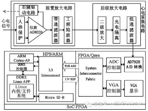
The ECG signal detection and monitoring system is a mixed analog and digital system, mainly divided into surface ECG signal acquisition circuits and a digital processing system centered around SoC FPGA. The acquisition circuit connects to medical lead wires through adhesive electrodes to pick up ECG signals. After amplification and analog filtering, the ECG signals enter the SoC FPGA, where an ARM embedded core on the HPS side controls A/D conversion based on a Linux application. The converted digital signals are displayed on the FPGA side via VGA, and the digital signals are transmitted to the HPS side for algorithm processing and storage on a MicroSD card. The hardware-software co-development approach of SoC FPGA is very convenient for both hardware design and the subsequent software development of ECG signal processing algorithms. The overall system architecture divided by functional modules is shown in the figure below.
The normal amplitude range of the ECG signal is 10 μV to 5 mV, with a typical value of 1 mV, and a frequency range of 0.05 to 100 Hz. Additionally, the ECG signal is very sensitive to noise. Therefore, the ECG signal acquisition circuit must have high input impedance, high common-mode rejection ratio, low noise, and low drift characteristics. The surface ECG acquisition circuit consists of a front-end amplifier circuit and a back-end amplifier circuit.
The front-end amplifier circuit mainly performs preliminary amplification and noise reduction on the acquired ECG signals to facilitate subsequent amplification and processing. The noise in the ECG signal mainly includes power frequency interference, electromyographic interference, baseline drift, and high-frequency noise. The front-end amplifier circuit consists of a primary amplifier circuit, a bandpass filter circuit, and a 50 Hz power frequency notch filter circuit. The primary amplifier circuit includes an input protection circuit, a right leg drive circuit, and an instrumentation amplifier circuit, as shown in the figure below.
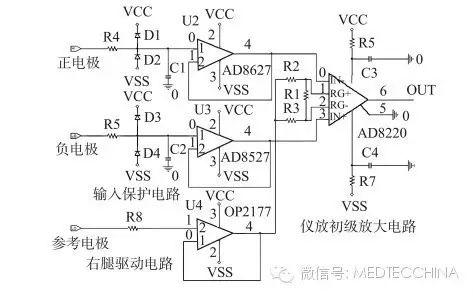
Since the system needs to connect to the surface acquisition signals, the issue of human protection during the signal acquisition process must be considered. Therefore, high-voltage transient voltage suppressors (TVS) diodes are chosen to protect both the human body and the circuit at the input stage of the acquisition circuit. The right leg drive circuit is used to connect the reference electrode during the acquisition of ECG signals, effectively eliminating common-mode interference present in the acquired signals. The instrumentation amplifier circuit completes the primary amplification of the ECG signal while also possessing high input impedance, high common-mode rejection ratio, low noise, and low drift characteristics. After comprehensive consideration, the AD8220 chip from ADI Company was selected for its precision instrumentation amplification. To prevent saturation distortion, the front-end gain is set to 20 times.
The ECG signals acquired by the circuit contain low-frequency baseline drift and high-frequency interference, as well as 50 Hz power frequency interference within the frequency range of the ECG signals. These noises significantly impact the extraction of ECG signals. A bandpass filter and a 50 Hz power frequency notch filter based on the general-purpose active filter module UAF42 have been designed. The passband of the bandpass filter circuit is 0.05 to 100 Hz, filtering out low-frequency interference such as baseline drift and high-frequency noise, while the power frequency notch filter effectively removes power frequency noise. The UAF42 allows for easy design of various types and frequency characteristics of filters; only the appropriate external resistor values need to be calculated, and simple connections can meet the design requirements, eliminating the need for capacitor and resistor selection and matching in the active filter design. The circuit diagram of the power frequency notch filter is shown in the figure below.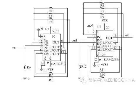 Using two UAF42 chips forms a 4-order notch filter to increase the notch depth, with a designed Q value of 50 and a 50 Hz notch depth of -110 dB. Compared to traditional twin-T notch filters, this notch filter allows the center frequency to be set during design, eliminating the need for debugging the notch center frequency. Furthermore, only resistors with calculated values need to be connected, avoiding the selection and matching of capacitors.
The back-end amplifier circuit consists of a two-stage amplifier circuit, an optical isolation circuit, and a low-pass filter circuit. Due to the gain values of the instrumentation amplifier and the bandpass filter in the front-end amplifier circuit not being set too high to avoid excessive noise interference and oscillation on effective signals, the overall gain magnitude is set between 1000 and 3500, and the amplification system’s gain will be achieved through multi-stage gain circuits. The two-stage amplifier circuit can reach the set gain value, while the operational amplifier is configured in a voltage feedback form to control the overall circuit gain. A low-cost precision capacitive linear optocoupler chip, ISO124, is chosen for the optical isolation circuit to achieve electrical isolation between the front and back circuits, avoiding feedback noise interference. The low-pass filter mainly eliminates high-frequency noise introduced by optical coupling, preventing high-frequency noise from the front circuit from entering the digital circuit board. The back-end amplifier circuit achieves electrical isolation between the analog circuit board and the digital circuit board.
Structure and Characteristics of SoC FPGA: This article uses Altera’s Cyclone V SoC FPGA based on 28 nm technology as the hardware design platform. This new type of SoC FPGA combines two discrete types of chips, integrating an ARM-based hard processor system (HPS) within the FPGA architecture.
Using Altera’s embedded design suite (EDS) SoC for hardware and software design development. The integrated Quartus II’s next-generation SOPC tool, Qsys, is used for hardware module design, which can automatically generate interconnection logic, connect intellectual property (IP) functions and subsystems. SoC EDS also provides tools to convert Qsys hardware system information into software development needs, linking hardware and software design together, supporting Linux application development, and using DS-5 for software design from boot code, kernel porting to Linux applications.
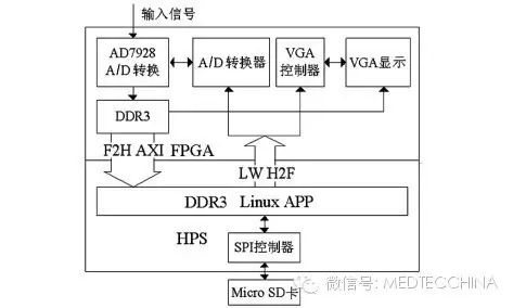
The digital system includes A/D conversion modules, VGA display modules, data storage modules, and algorithm processing modules. The HPS and other hardware modules in the SoC FPGA can be configured via Qsys, and hardware design is conducted using Quartus II. Qsys and Quartus II compilation can produce the information files needed for software design. The A/D converter used in the system is ADI’s 8-channel, 12-bit high-precision low-power A/D conversion chip AD7928, with a conversion rate of 1 MSPS. The American Heart Association recommends a sampling rate of 500 Hz, but in practice, different applications have different sampling rates, generally between 125 and 1000 Hz. During monitoring, 200 Hz or 250 Hz is often used, while auxiliary analysis typically employs 400 to 500 Hz, and ECG HOLTER generally takes 125 to 200 Hz; this system adopts 200 Hz. Programs are written to control A/D conversion and data buffering, generating the line and column synchronization signals needed for VGA control, as well as blanking signals, clock signals, and RGB signals to ensure the screen works correctly. The embedded Linux file system supports writing and reading data from the Micro SD card, transmitting digital signals to the HPS side via the AXI bridge, and the software engineering implements ECG signal algorithm processing and Micro SD card data storage. The structural diagram of the system’s digital part is shown in the figure below.
After completing the system design, the front-end acquisition circuit and the overall system were debugged and tested. Three-lead method using medical adhesive Ag/AgCl ECG electrodes was employed, connected to the ECG signal acquisition system for testing.
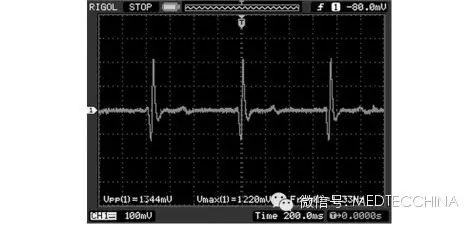
The subject wears ECG electrodes, connected to the analog front-end acquisition circuit with medical lead wires, and the back end is connected to an oscilloscope. Once the signal stabilizes, the ECG signal waveform can be observed on the oscilloscope. The figure below shows the actual test waveform of the analog front-end circuit.
Connecting the overall system and running the software engineering, the system stores a segment of ECG signals, and after taking out the Micro SD card, the stored data is read to restore the ECG signal waveform as shown in the figure below.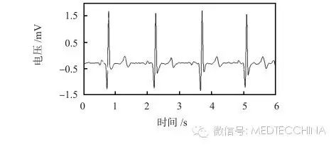
ECG signal algorithm processing has become increasingly widespread with the application of intelligent healthcare. In specific application environments such as health monitoring and disease diagnosis, traditional algorithm processing is generally hardware-based, which tends to be more challenging and resource-intensive. The porting of embedded Linux systems greatly facilitates the software implementation of ECG signal algorithm processing. In the software engineering, wavelet denoising and QRS wave detection of ECG signals have been implemented.
Wavelet analysis is employed for ECG signal denoising. Wavelet analysis can simultaneously analyze signals in both time and frequency domains, providing multi-resolution analysis functions, effectively distinguishing signal abrupt changes from noise at different decomposition levels. After performing wavelet decomposition on the original ECG signal containing noise, the noise part mainly concentrates in the high-frequency wavelet coefficients, while the wavelet coefficients containing useful signals have larger magnitudes but fewer counts; conversely, the wavelet coefficients corresponding to noise have smaller magnitudes but more counts. Based on these characteristics, unbiased likelihood estimation thresholds are selected to process the wavelet coefficients, followed by signal reconstruction to achieve the denoising purpose. The figure below compares the ECG signal before and after wavelet denoising, achieving a signal-to-noise ratio of up to 121 dB.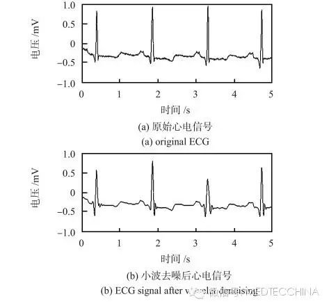
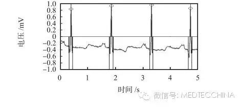
According to the theory of wavelet transform, the singular points of the signal correspond to a positive and negative mode maxima of its wavelet transform, with their positions corresponding to the zero-crossing points of the positive and negative mode maxima. The specific algorithm finds the maximum modulus of the wavelet transform; when the calculated signal modulus exceeds a certain threshold, it is determined as a QRS wave group. Simultaneously, this threshold is adaptively updated based on computed results. After identifying the QRS wave group, zero-crossing detection can determine the specific R-wave position. The figure below shows the detection of the ECG signal QRS wave group and the location of the R-wave peak.
 After detecting features such as the R-wave peaks from the ECG signal using wavelet analysis, these extracted feature values can be used for pattern recognition and classification, for example, using BP neural networks to classify the morphology of the ST segment of the electrocardiogram.
The ECG signal detection system designed based on SoC FPGA can effectively acquire ECG signals, achieving extraction, display, storage, and processing of ECG signals. Tests indicate that the system’s analog front-end circuit can acquire relatively clear ECG signals amplified to appropriate levels, and overall system testing proves the feasibility of the design. The hardware-software combined development approach of SoC FPGA enables algorithm processing of ECG signals, making the design more flexible and providing convenience for ECG signal processing and analysis, as well as potential for the realization of intelligent healthcare.
*Cited from: Jiang Peihai, Huang Qijun, Chang Sheng, Wang Hao, He Jin
“Design of ECG Signal Detection System Based on SoC FPGA”