This article will introduce how to desolder Flash chips, design and create corresponding breakout boards. It covers simple and effective attack methods on the non-volatile storage of embedded devices. These attacks include:
-
Reading the contents of the storage chip
-
Modifying the contents of the chip
-
Monitoring read operations on the storage chip and modifying remotely (man-in-the-middle attack)
Imagine, when you open an embedded product, but are blocked from accessing the Flash, your curiosity must lead you to want to explore it.
So, let’s get started.
Desoldering the Flash Chip
To read the contents of the Flash chip, there are two basic approaches:
-
Directly connecting wires to the chip’s pins
-
Removing the chip and inserting it into another board
The Flash discussed here is in a BGA (Ball Grid Array) package—without exposed pins. Therefore, the only option is to desolder it.
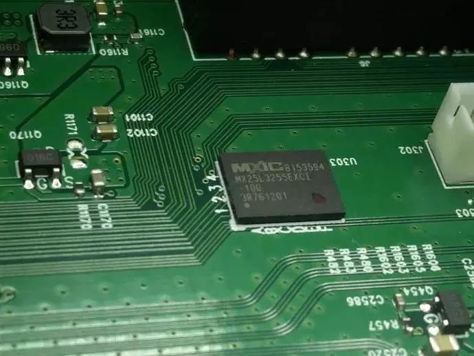
Figure: Target Chip
Advantages of the Desoldering Method:
-
Avoids affecting other components on the circuit board;
-
Allows easy visibility of the wiring on the bottom of the chip;
-
Can replace the original chip with another chip or microcontroller.
Some Inconveniences:
-
The circuit cannot operate without the complete component;
-
During disassembly, some adjacent components may be damaged;
-
If not handled properly, the Flash itself may be destroyed.
OK, desoldering, right? Look, the hot air gun shown in the picture is simply a magical tool. Just heat the area around the chip, and you can easily remove it:
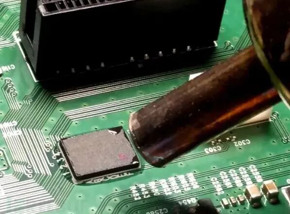
Figure: Hot Air Gun Desoldering
This method is simple and quick but may harm innocent components—so be very careful.
The next image shows the PCB wiring after the chip has been removed. Observe the picture and guess that the two columns of pins at the bottom are empty pins because they are not connected to the circuit at all.
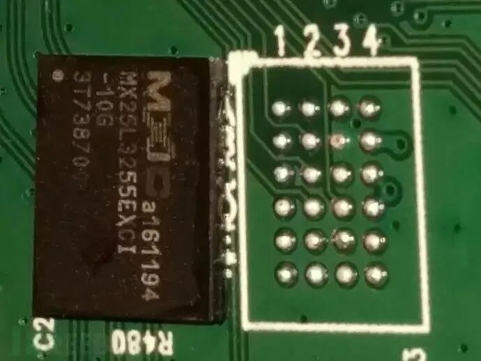
Figure: After Desoldering
Custom Breakout Board with KiCAD
What should we do now? The BGA package is a complete mess, and we still cannot connect wires externally.
One feasible method is to create a breakout board. Typically, a breakout board mirrors the positions of all the chip’s pins, allowing the chip’s pins to be brought out.
To do this, we first need to gather relevant information about the chip. In most cases, the chip model is printed on the chip, making it easy to identify. As shown in the image above, the first line on the chip reads MXIC, representing Macronix International, and the second line shows the specific chip model MX25L3255EXCI datasheet. Below is the datasheet information:
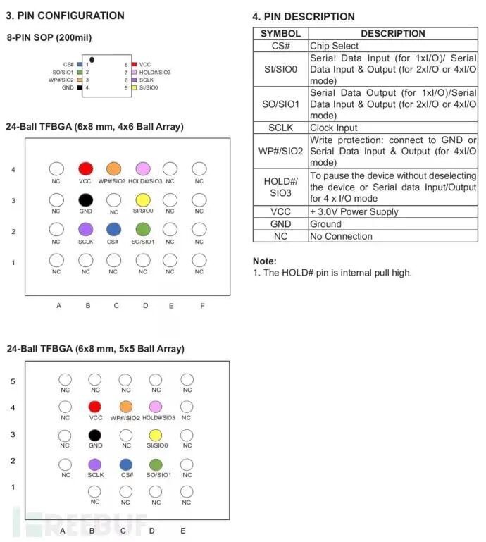
Figure: Pin Layout
The PCB design can be accomplished using KiCAD, a commonly used EDA software.
The design process for the breakout board is similar to that of other PCBs:
-
Create a new circuit board, draw the circuit schematic, and specify the exact model of the components
-
Determine the specific dimensions of the chip
Based on the previous datasheet information, we add a 4×6 grid for the entire chip’s BGA package and two 1×4 grids as connection posts for the chip’s 8 active pins. The final step is to connect these components with traces:
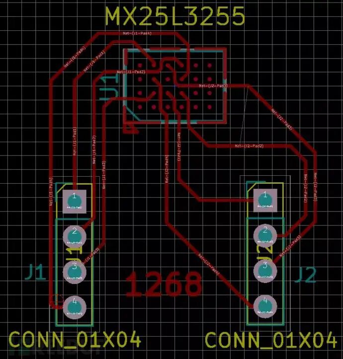
Figure: Step 2
The design of the breakout board is now complete; the next step is how to turn the design into a PCB.
PCB Fabrication
A PCB is like a sandwich made of two layers of copper and one layer of substrate, with traces distributed on the copper surface.
According to the fabrication process, it can be divided into:
-
Etching Method
-
CNC Milling Method
Below are the specific steps for both methods.
Etching Method
Etching is the process of gradually removing copper using chemical agents. We first protect the traces and the copper we want to keep on the copper-clad board with ink.
1. First, use the heat transfer method to create the PCB. The PCB circuit diagram is printed on glossy paper using a laser printer. Then, the glossy paper is pressed tightly against the copper-clad board, heated, and pressure is applied to transfer the circuit diagram from the glossy paper to the copper-clad board. Typically, this process can be completed with an iron, but a dedicated press will make the heating and pressure more uniform, making it easier to succeed.
2. Next is the etching, where the entire PCB board is immersed in an etching solution to remove the excess copper.
The etched breakout board still has the transferred ink powder on it:
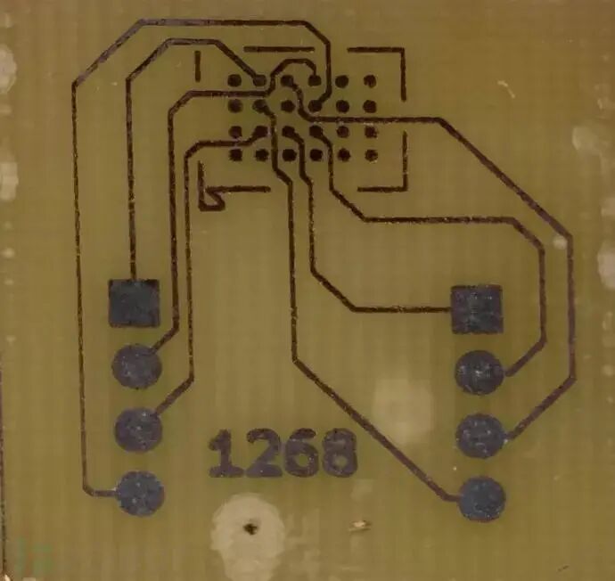
Figure: Step 3
After removing the ink powder:
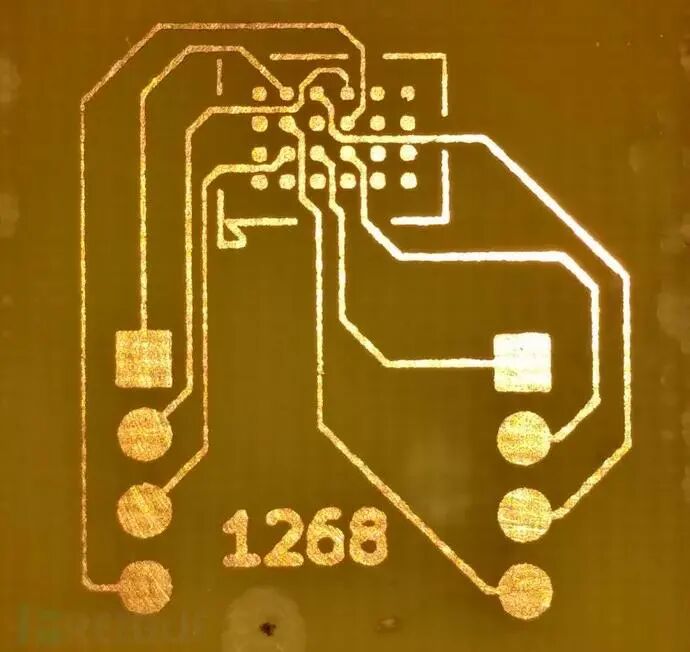
Figure: Step 4
Now we can prepare for manual soldering. Micro soldering is similar to normal soldering, but the components are extremely small, so a microscope is needed.
Additionally, traditional soldering uses wire solder, while BGA micro soldering uses solder balls.
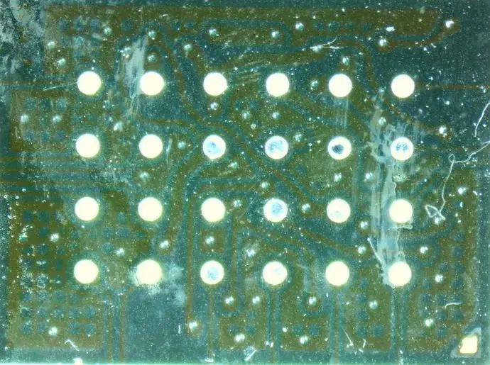
Figure: Step 5
Next, start reflowing the solder balls:
-
Place a new solder ball in the recess, heat it to melt the solder ball;
-
Align the chip and the board;
-
Reflow.
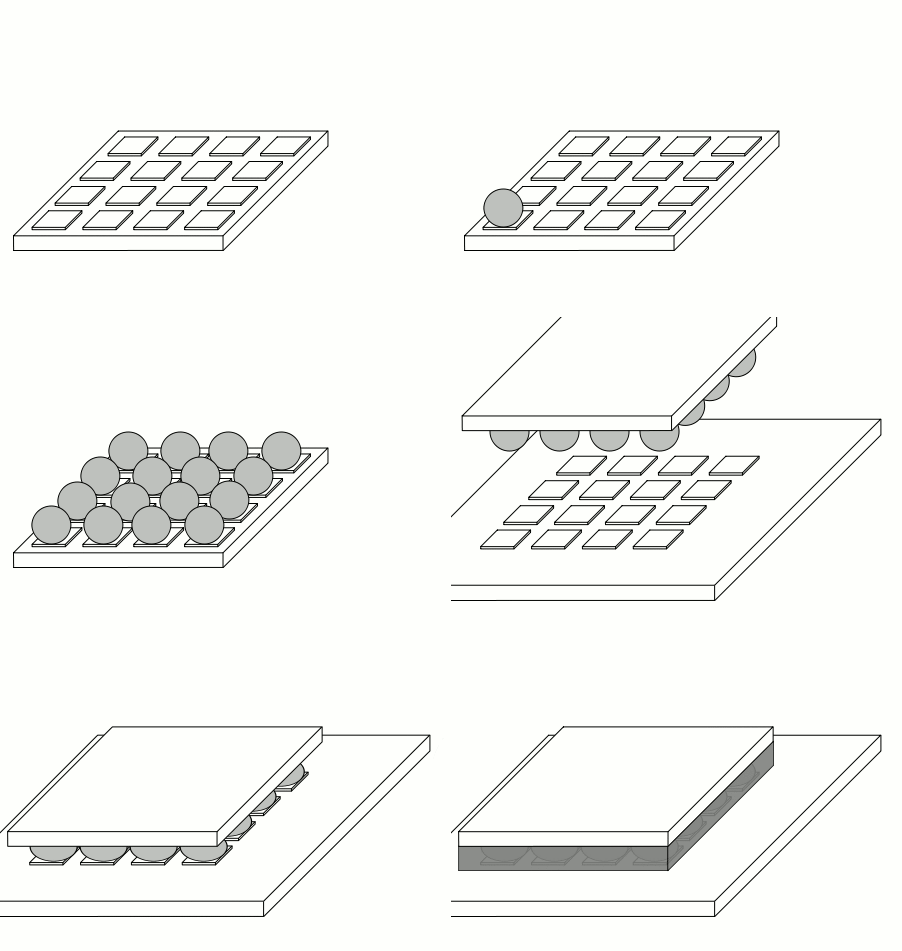
Figure: Step 6
Reflowing of the solder balls is complete:
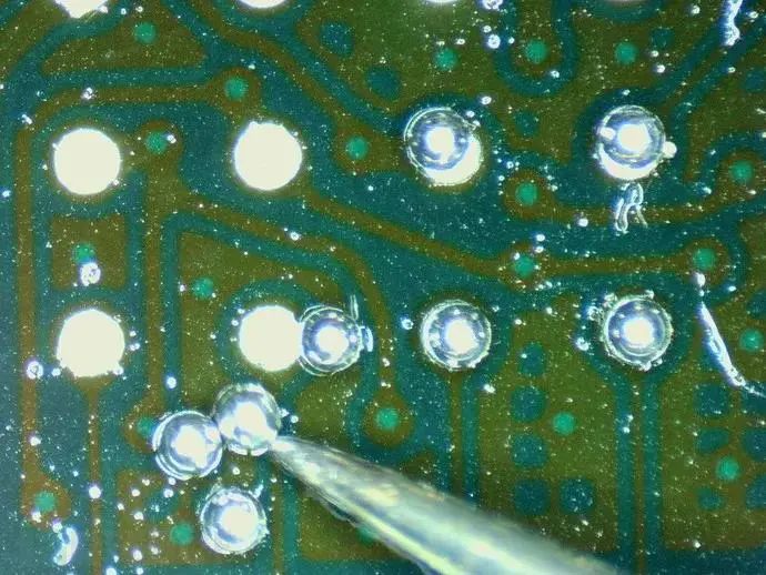
Figure: Step 7
The final result after soldering the chip:
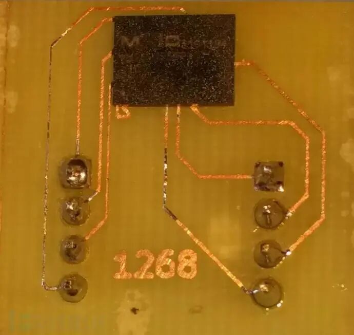
Figure: Step 8
CNC Milling
As an alternative method, CNC milling simply isolates the required traces and remaining copper.
(1) A 5X5 BGA is typically used for making PCBs, while a 4X6 is commonly used for breakout boards. We designed the 5X5 so that the breakout board can be directly plugged into the ZIF socket of a universal EEPROM programmer, as shown in the circuit schematic below:
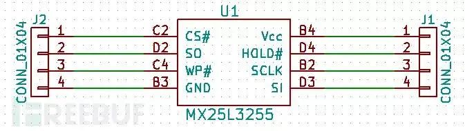
Figure: Step 9
(2) The chip size is the same as the previously designed 4X6, but the grid has changed to 5X5, and the wiring on the board is slightly more complex:
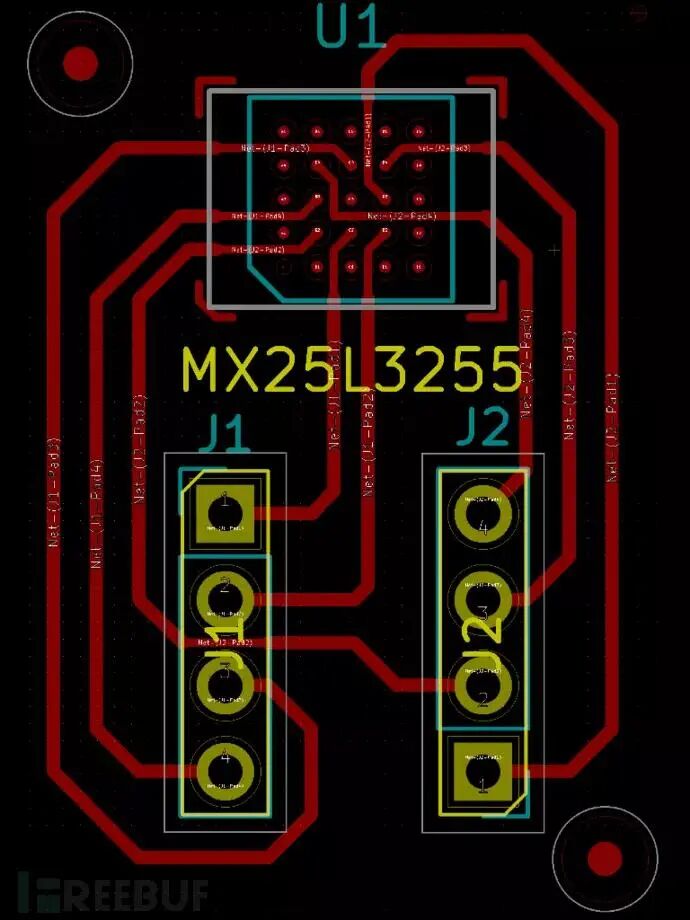
Figure: Step 10
(3) Since KiCAD cannot directly generate target files compatible with CNC milling, we use Flatcam to receive Gerber files and determine the paths for isolating traces:
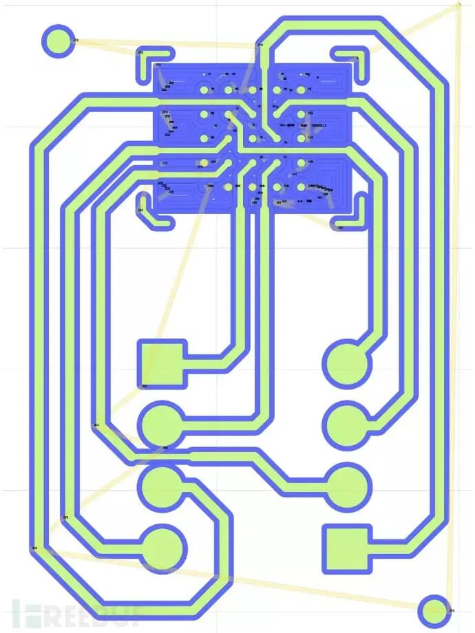
Figure: Step 11
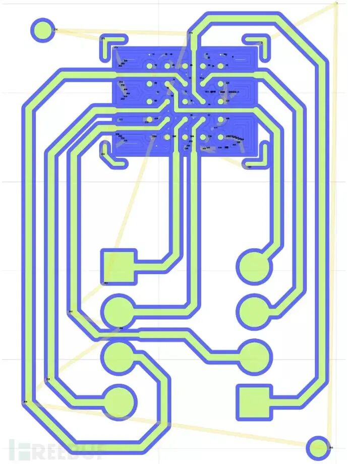
Figure: Step 12
(4) Next, import the generated STL file into bCNC—the terminal control program for CNC milling, as shown in the image below:
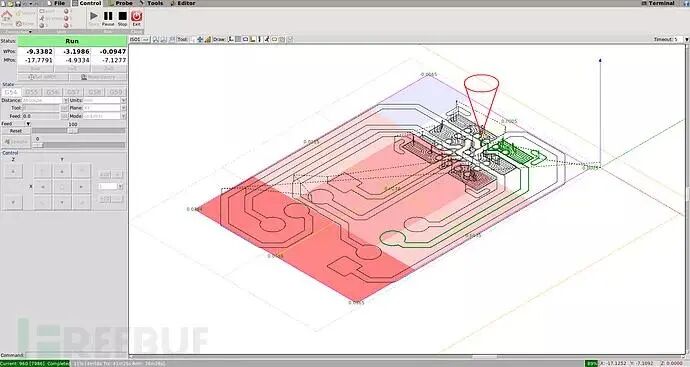
Figure: Step 13
During the engraving process:
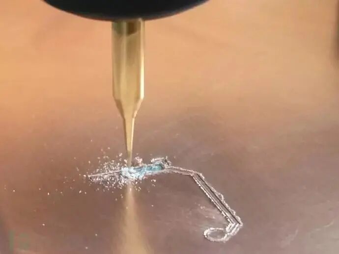
Figure: Step 14
(5) The board engraving is complete:
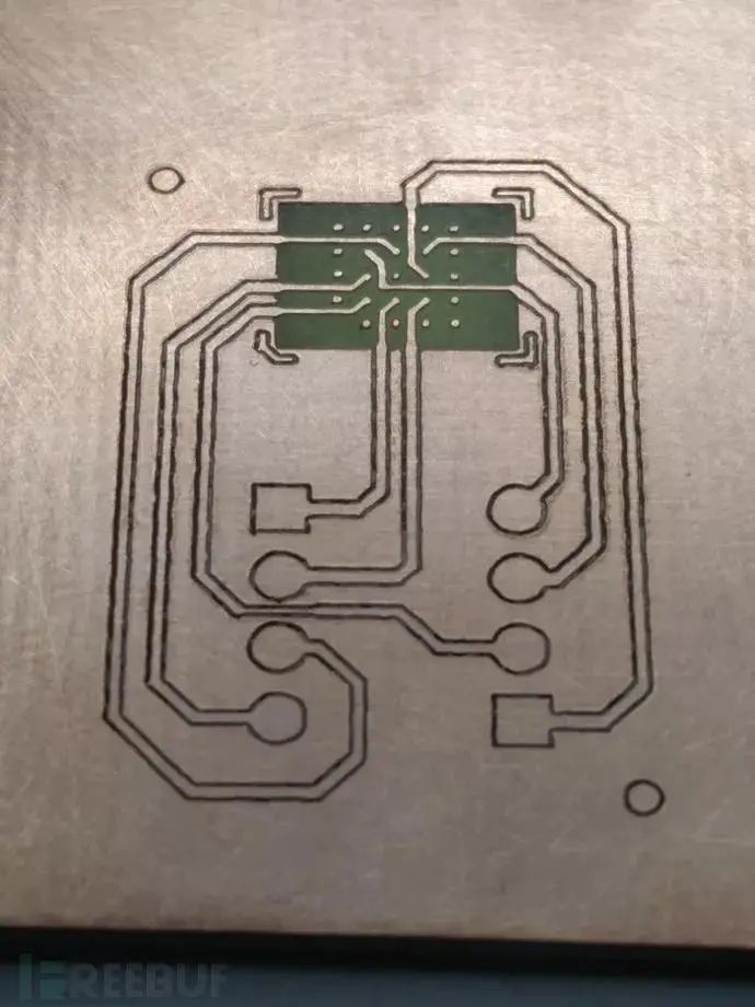
Step: 15
Final result:
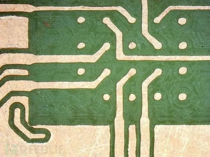
Figure: Step 16
(6) The next step is to apply a solder mask to protect the copper from oxidation and cure it with a UV lamp:
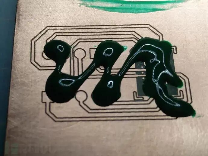
Figure: Step 17
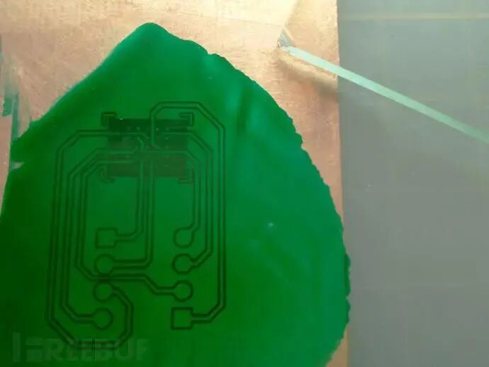
Figure: Step 18
(7) The solder mask covers the copper pads of the BGA and the 1X4 connection posts, and we need to scrape off this thin layer to expose the copper pads:
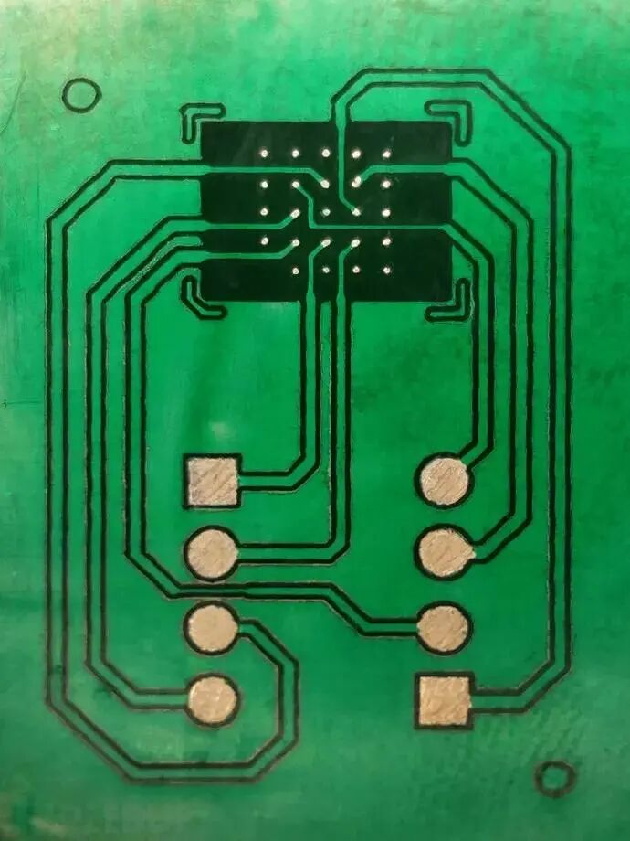
Figure: Step 19
(8) Solder the various nodes:
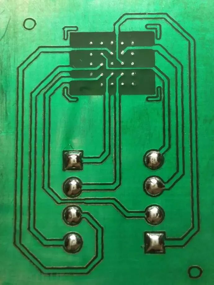
Figure: Step 20
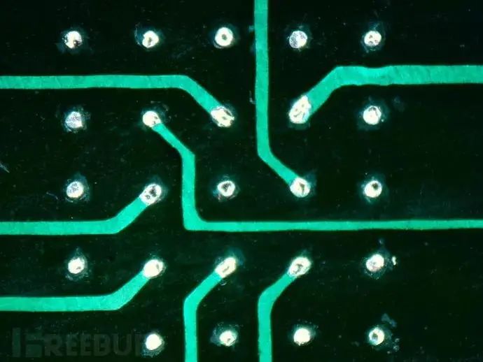
Figure: Step 21
(9) Back to CNC milling, drill holes and cut the edges of the PCB:
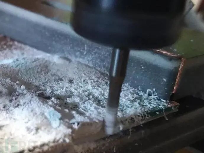
Figure: Step 22
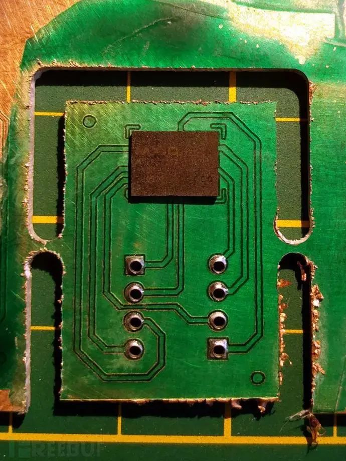
Figure: Step 23
(10) The final product, the BGA is soldered onto the board, ready to be plugged into the EEPROM programmer:
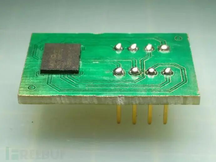
Figure: Step 24
Conclusion
We have learned how to desolder Flash chips, design PCBs, and the two different methods of PCB fabrication.