Today, semiconductor companies face severe challenges related to shrinking technology nodes, expanding design scales, and broadening system scales (known as the “three major scaling challenges”). These challenges have a wide-ranging impact on design development, manufacturing, and functional operations, all of which affect the company’s operating profits. At the same time, the complexity of large System on Chip (SoC) design is increasing day by day, posing even more severe challenges to all IC design disciplines, including Design for Testability (DFT).The consequences of traditional DFT methods include:delayed time to market, testing costs exceeding expectations, low chip quality, slow yield improvement, and inability to maintain device performance throughout the lifecycle. There are many reasons for this situation, but all are related to the three major scaling challenges. Therefore, to improve the efficiency of DFT and enhance the competitive advantage of companies, the industry urgently needs smarter DFT solutions.As a market leader in SoC chip DFT testing, Siemens EDA’s Tessent software provides a complete chip testing and yield analysis platform, along with top-notch software and IP to address these challenges.The Tessent product line spans the entire chip product lifecycle—from wafer, package testing to aging, in-system, and field testing. For example, the Tessent streaming scan network (SSN) can help DFT engineers shorten test times and reduce test data volume; Tessent™ LogicBIST provides high-quality in-system test solutions for safety-critical devices such as automotive ICs and medical ICs; Tessent supports the security, stability, and reliability of automotive OTA updates.
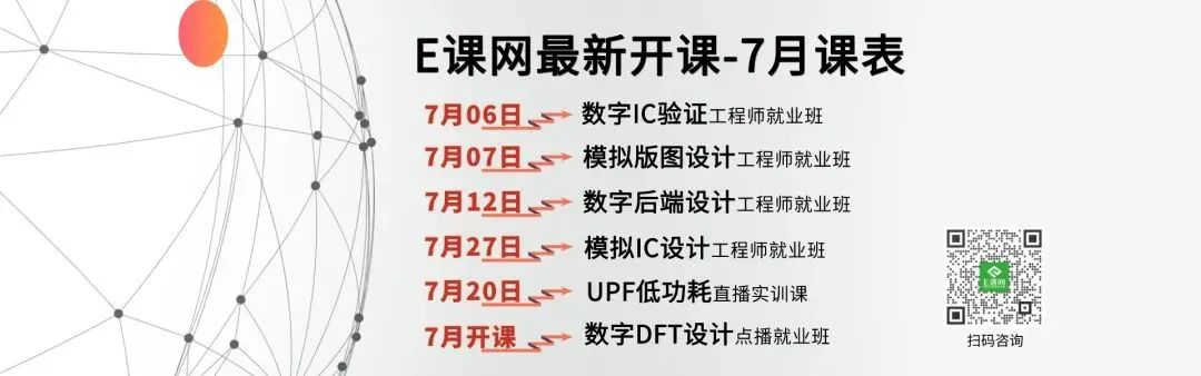
This July, the E Course Network DFT Design Engineer On-Demand Course is launched! It delves into DFT professional theory, with modular courses designed and refined by experienced engineers over more than 10 years; the teaching methods are diverse, with expert instructors combining practice to meet the needs of students with different backgrounds, compact and to the point; you can listen anytime, anywhere, without being restricted by time, location, or network, saying goodbye to video lag and delays; click where you don’t understand! If you want to learn about the on-demand course and study efficiently together, please scan the code for consultation.
 To assist chip engineers in completing their design work more efficiently and accelerate time to market, Siemens EDA has launched several technical resources for reference and learning.Scan the QR code below, fill it out, and you can download the materials.

Reference Materials:“Addressing Scaling Challenges for Wafer Success”“Chip Testing for Safety-Critical Applications”“Bottom-Up DFT Methods”“Updating, Monitoring, and Controlling Automotive Devices Using Over-the-Air Download Technology”“Automotive Safety Island ISO 26262 Edge Testing, Safety, and Security Data Management”
Recommended Reading
 The live broadcast room almost ignited the IC circle! Netizens said, “Even college teachers are getting involved.”The Moore Elite & Chongqing University of Posts and Telecommunications Integrated Circuit Design Summer Training Class has successfully concluded.This summer, the Mee Talent Cloud Training Base officially opened in Zhangjiang!Hot hot hot! “High-temperature” warning, UPF has been upgraded to support longer battery life.Beijing, Shanghai, Shenzhen, Chengdu, Wuhan, Hefei, Chongqing | Major Chip Design Companies (Fabless)My dream in July: to become a DFT expert and surpass 98% of competitors.Domestic chip companies’ performance forecasts show a stark contrast.Technical resources | Linux operation demonstration……


E Course Network (www.eecourse.com) is a professional integrated circuit education platform under Moore Elite, dedicated to cultivating high-quality integrated circuit professionals in the semiconductor industry. The platform is oriented towards the job demands of integrated circuit companies and provides a training platform that fits the corporate environment, rapidly training students to meet corporate needs through both online and offline training methods.
The E Course Network boasts a mature training platform, a complete curriculum system, and a strong faculty. It has planned a premium course system of 168 courses in China’s semiconductor industry, covering the entire integrated circuit industry chain, and has four offline training bases. To date, it has deeply trained a total of 15,367 people and directly delivered 4,476 professionals to the industry. It has established deep cooperation with 143 universities and has held 240 corporate special IC training sessions.