In the development of high-speed hardware products, PCB materials serve as the actual carrier of hardware design. Particularly in high-speed product design, the performance of the material often determines the deviation between the actual maximum transmission rate and the theoretical maximum transmission rate. In hardware product design, issues such as “PCB material downgrade leading to design speed reduction” or “choosing overly high-grade PCB materials leading to high costs” are frequently encountered. During the hardware design process, it is common to evaluate the selection of materials based on the routing speed, as different types and parameters of materials directly affect the performance, reliability, and cost of the circuit board. So how can we reasonably select materials? This article will analyze this issue from the perspective of Signal Integrity (SI).
Introduction to Material Parameters
We all know that for PCB materials, the most critical parameters are the relative permittivity (Dk) and the dissipation factor (Df). These two parameters directly affect the electrical performance and signal transmission characteristics of the circuit board (such as characteristic impedance and signal loss). However, as signal rates increase, for example, when the signal single-lane rate is 56Gbps or 112Gbps, the glass fiber cloth, copper foil roughness, and green oil used in the material will greatly affect the signal transmission characteristics.
- Dielectric Constant (Dk)
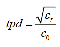
The dielectric constant (Dk) refers to the ability of a material to store electrical energy under the influence of an electric field. It is an inherent property of the material and is usually dimensionless. The magnitude of the dielectric constant reflects the material’s capacitance capability relative to vacuum. The dielectric constant of vacuum is defined as 1, while other materials typically have a dielectric constant greater than 1. For example, the commonly used FR4 material in PCB product design has a dielectric constant of about 4.2. In simple terms, the size of the dielectric constant directly affects the impedance of the routing. For instance, when the routing impedance is 50Ω, using FR4 material will result in wider routing compared to high-speed materials (M4). If there are constraints on routing width in the design, the dielectric constant can be adjusted to flexibly change the line width. Additionally, the speed of signal propagation in the medium is inversely proportional to the dielectric constant. A lower dielectric constant helps to increase the signal propagation speed. Therefore, high-speed materials typically have a dielectric constant (2.8-3.5) that is lower than that of low-speed materials (3.8-4.5). For instance, the dielectric constant of common M4 materials is around 3.8, while that of FR4 is about 4.0, and M6 materials have a dielectric constant of around 3.2 (note that the dielectric constants of different material manufacturers may vary slightly). The speed of signal propagation in PCB materials can be estimated using the following formula.
- Dissipation Factor (Df)
The dissipation factor (Df), also known as the dielectric loss or loss factor, measures the ability of dielectric materials to dissipate energy under the influence of an electric field. It represents the ratio of dielectric loss to energy storage capability and is an important indicator of material electrical performance. The lower the value of the dissipation factor, the smaller the dielectric loss of the material, and the lower the signal transmission loss. It is important to note that the dissipation factor directly affects the signal attenuation of the circuit board, especially in scenarios with signal rates of 25Gbps, 56Gbps, and 112Gbps, where the dissipation factor is a significant factor affecting signal attenuation (insertion loss).
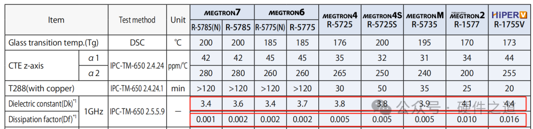
The above image shows the Dk and Df values of Panasonic’s M series materials, clearly indicating that as the material grade increases, both the Dk and Df values decrease. The goal of having a smaller Dk value is to enhance the signal transmission speed in the PCB material, while a smaller Df value aims to reduce signal loss in the material.
- Glass Transition Temperature (Tg)
Tg is one of the important parameters of PCB materials, indicating the temperature at which the material transitions from a glassy state (hard and brittle) to a rubbery state (soft and ductile). The Tg value directly affects the thermal and mechanical performance of the PCB. High Tg materials can maintain stable physical and mechanical properties in high-temperature environments, reducing thermal expansion and contraction, thereby improving PCB reliability. Generally, the selection of the Tg parameter is based on the application environment temperature and the maximum temperature that the board can reach during operation. Taking the commonly used FR4 material from Jialichuang as an example, the price of similar materials varies according to different Tg values.
Introduction to High-Speed Materials
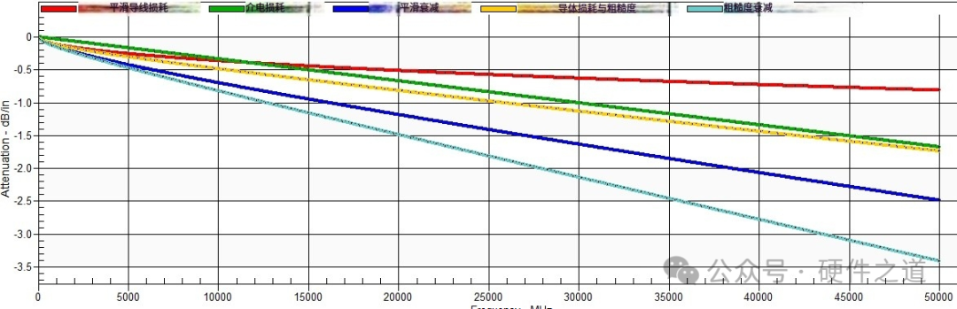
Regarding high-speed PCB materials, domestic PCB material suppliers are currently benchmarking against Panasonic’s PCB materials, which are regarded as the industry standard due to their excellent electrical, thermal, and mechanical performance. In the fields of high-speed digital and high-frequency applications, common Panasonic materials include M4, M6, and M8 types. The higher the grade of the material, the lower the losses associated with it. The losses of different series of Panasonic materials are also referenced in the following image:

To reasonably select PCB materials based on the maximum signal rate of the board, it is necessary to comprehensively consider parameters such as Df, Dk, the type of glass fiber cloth, and the roughness of the copper foil. A rough rule of thumb is that for signal rates below 10Gbps, FR4 materials can be used; for signal rates around 25Gbps, M4 grade materials must be used; for signal rates above 56Gbps, M6 grade materials must be used; and for signal rates above 112Gbps, M7 grade materials must be used. This rule of thumb has a constraint that the length of PCB routing should not be too long or too short. Generally speaking, the losses associated with PCB materials will rapidly increase with the signal frequency. However, it is certain that for signal rates above 25Gbps, unless the routing is very short, M4 grade materials or higher must be used, as the higher the material grade, the different types of glass fiber cloth and copper foil roughness are critical parameters in the high-speed domain. From the perspective of SI, when high-speed signals are transmitted in PCB materials, various losses occur during the signal transmission process, which can affect signal integrity and circuit performance.
- Dielectric Loss
We refer to the energy attenuation caused by the loss of the dielectric material during signal transmission as dielectric loss. Dielectric loss is particularly significant in high-frequency applications and has a crucial impact on signal integrity and transmission performance. During the design process, the dielectric constant (Dk) and dissipation factor (Df) of PCB materials influence dielectric loss. Materials with high Dk and high Df will increase the dielectric loss of the signal.
- Conductor Loss
When signals are transmitted in PCB materials, as the frequency of the signal increases, the skin effect occurs, meaning that electromagnetic signals will be transmitted along the surface of the copper foil in the material. The roughness of the copper foil in low-speed materials is relatively poor compared to high-speed materials. Therefore, when high-speed signals are transmitted using low-speed materials, conductor loss becomes a serious issue. In simple terms, the factors affecting conductor loss mainly include the resistance of the conductor and surface roughness. The resistance of the conductor increases with frequency, and when high-frequency signals are transmitted on the surface of the conductor, surface roughness will increase signal loss (skin effect).
Factors Affecting Signal Transmission
In addition to the common parameters mentioned above, such as Df and Dk, other factors affecting high-speed signal transmission include the type of glass fiber cloth and the roughness of the copper foil.
- Glass Fiber Effect
The impact of glass fiber cloth is often described using the term “glass fiber effect”. The glass fiber effect refers to the changes in signal propagation speed due to microscopic inhomogeneities (especially the presence of glass fiber cloth) along the signal path during high-speed signal transmission through the PCB, leading to signal integrity issues. This effect is particularly important in high-speed signal design, as it can cause signal distortion, increased jitter, crosstalk, and higher bit error rates. The actual impact of the glass fiber effect can be illustrated as follows. Due to the dielectric materials used in the PCB manufacturing process, which are made from woven glass fiber yarns and impregnated with epoxy resin, they become uneven. If high-speed differential signals are not constrained during layout, it can lead to routing distributed across different dielectric constants on the PCB plane, resulting in different signal transmission delays, causing differential voltage misalignment, common-mode voltage deviations, and differential signal mode conversion deviations, thus failing to produce the ideal waveform.
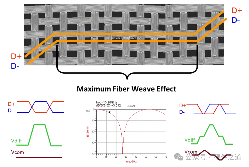
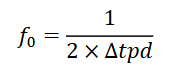
Generally speaking, good materials appear denser in the manufacturing process, and the average Dk value of the overall material tends to be more stable. 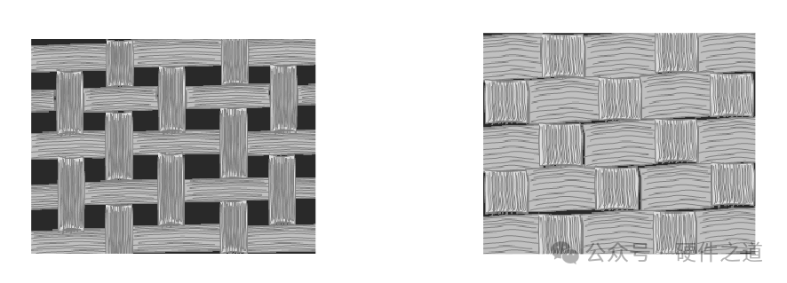 From the perspective of SI, due to the routing of high-speed differential signals on the material, the influence of the woven cloth leads to deviations in the dielectric constants between the two lines, resulting in different propagation delays of the signals on the PCB, thus causing timing offsets. The internal timing offsets of differential signals can lead to differential insertion loss and resonance. The following formula can be used to roughly estimate the resonance frequency point.
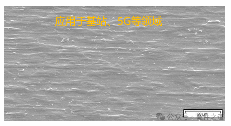
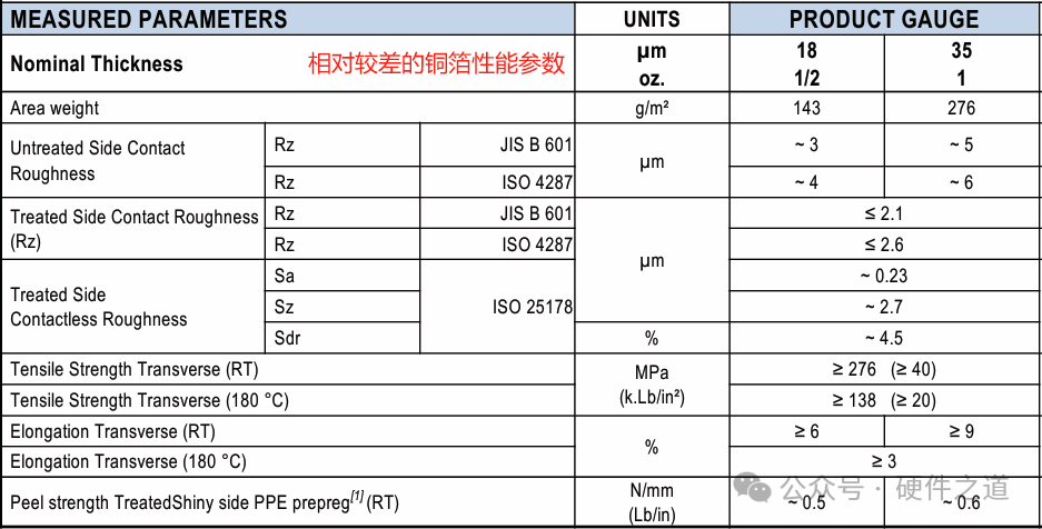
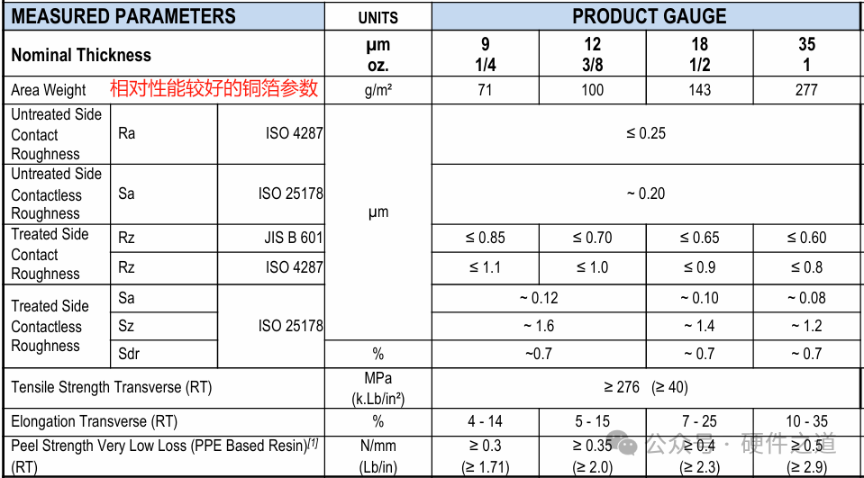
- Copper Foil Roughness In the PCB manufacturing process, to improve the adhesion of the copper foil to the PCB substrate, the surface of the copper foil is usually roughened. These treatments include sandblasting, electroplating, etc., aimed at increasing the microscopic unevenness of the copper foil surface, thereby enhancing the resin’s wettability and adhesion, and reducing the risk of interlayer delamination. Additionally, since copper foil is often obtained through electrolysis during manufacturing, the electrolyte and production methods can lead to irregularities on the copper foil surface, which are one source of roughness. However, as the signal transmission frequency increases, the roughness of the copper foil can affect the characteristic impedance of the transmission line. If the surface of the copper foil is uneven, it can lead to impedance inconsistencies, causing signal reflections and jitter, thus affecting signal integrity. Furthermore, increased copper foil roughness increases the path length of the conductor surface, leading to signal delays, which need to be carefully considered in high-speed signal design, especially in applications at 56Gbps and 112Gbps. If the roughness of the copper foil is not evaluated, it can lead to disastrous consequences for the design.
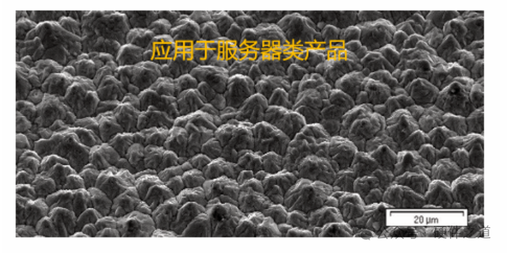
For good materials, the copper foil roughness is often smaller. Generally speaking, the copper foil used in materials can be classified based on roughness levels: standard roughness (SP), low roughness (LP), ultra-low roughness (ULP), and very low roughness (VLP). Taking two conventional types of copper foil as examples (both used in high-speed digital fields), the differences in copper foil roughness can be clearly seen at the same magnification. Similarly, in higher frequency and high-speed application scenarios, the impact of two types of copper foil on signal insertion loss and return loss is also significant.
Comparison and Analysis of Simulation Models
Taking the PCIe Gen5 simulation model as an example, we compare the effects of copper foil roughness of 35um (FR4 material) and 5um (M6G material) on the signal (subsequent sections will address the SI chapters corresponding to material characteristics at rates above 50Gbps).
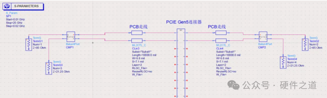
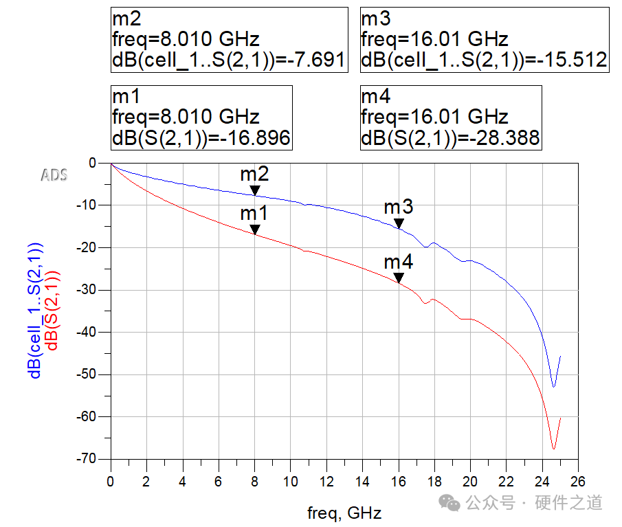
From the above images, it can be seen that when the link operates at PCIe Gen4 rates, the insertion loss due to copper foil roughness is close to 9.2dB (under the same Dk and Df conditions). When the link operates at PCIe Gen5 rates, the insertion loss due to copper foil roughness is close to 12.8dB (under the same Dk and Df conditions). As noted in the section “How to Analyze PCIe Gen5 Interface Design from the SI Perspective”, the total loss of the PCIe link must be less than 36dB (without using a retimer). If the roughness of the copper foil is not constrained during the design process, it will adversely affect the transmission distance and signal quality of the entire link.
Completing a good high-speed hardware product design requires equal importance on circuit design and PCB materials. Choosing the right PCB material often determines the overall design quality and cost advantages of the product.