Stage One

1
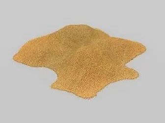
Sand
Silicon is the second most abundant element in the Earth’s crust, and sand (especially quartz) contains up to 25% silicon in the form of silicon dioxide (SiO2), which serves as the foundation for the semiconductor manufacturing industry.
2
Silicon Smelting
12-inch/300mm wafer level. Through multiple purification steps, silicon of semiconductor manufacturing quality is obtained, known as electronic-grade silicon (EGS), with at most one impurity atom for every million silicon atoms.

Stage Two

1
Silicon Ingot Cutting
Cut into circular individual silicon wafers, commonly referred to as wafers.
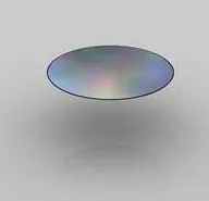
2
Wafer
The cut wafers become nearly flawless after polishing, with surfaces that can even serve as mirrors.

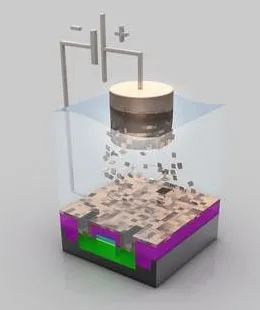
Stage Three

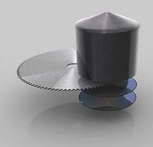
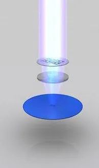
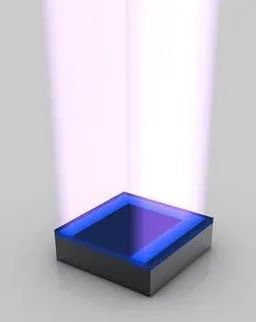
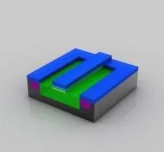
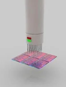
1
Photo Resist
The blue portion in the image is the photoresist liquid poured onto the wafer during its rotation, similar to the traditional film-making process. The rotation allows the photoresist to spread very thin and evenly.

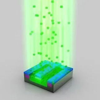
2
Photolithography
The photoresist layer is then exposed to ultraviolet (UV) light through a mask, becoming soluble. The chemical reaction during this process is similar to the moment a mechanical camera shutter is pressed. The mask contains pre-designed circuit patterns, and the UV light passing through it will form each layer of the microprocessor’s circuit patterns. Generally, the circuit patterns obtained on the wafer are one-fourth of those on the mask.
This results in transistors at the scale of 50-200 nanometers. A single wafer can yield hundreds of processors, but from here we narrow the focus to one, demonstrating how transistors and other components are made. Transistors act as switches, controlling the direction of current.
Today’s transistors are so small that approximately 30 million can fit on a pinhead.

Stage Four

1
Dissolving Photo Resist
The photoresist exposed to UV light during the lithography process is dissolved, leaving a pattern that matches the mask.
2
Etching
Chemicals are used to dissolve the exposed portions of the wafer, while the remaining photoresist protects the areas that should not be etched.
3
Removing Photo Resist
After etching is complete, the photoresist has fulfilled its mission and is completely removed, revealing the designed circuit pattern.
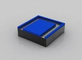
Stage Five
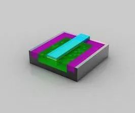
1
Photo Resist
Another layer of photoresist (the blue portion) is applied, followed by photolithography, and the exposed parts are washed away. The remaining photoresist continues to protect the areas that will not undergo ion implantation.
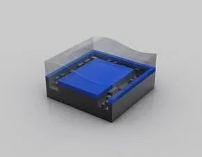
2
Ion Implantation
In a vacuum system, ions of doped atoms are accelerated and injected into solid materials, forming a special implanted layer in the injected area and altering the conductivity of the silicon in those regions. After acceleration by an electric field, the injected ion stream can exceed speeds of 300,000 kilometers per hour.
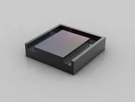
3
Removing Photo Resist
After ion implantation is complete, the photoresist is also removed, and the implanted area (green part) has been doped with different atoms. Note that the green color at this point is different from before.

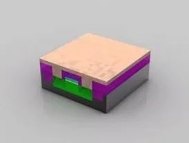
Stage Six

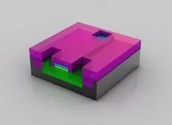
1
Transistor Ready
At this point, the transistors are basically complete. Three holes are etched into the insulating material (magenta) and filled with copper for interconnection with other transistors.
2
Electroplating
A layer of copper sulfate is electroplated onto the wafer, depositing copper ions onto the transistors. Copper ions flow from the anode to the cathode.
3
Removing Photo Resist
After electroplating, copper ions are deposited on the wafer’s surface, forming a thin layer of copper.

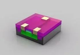
Stage Seven

1
Polishing
The excess copper is polished off, which means polishing the surface of the wafer.
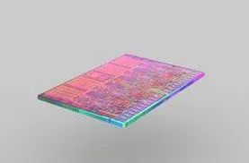
2
Metal Layer
At the transistor level, a combination of six transistors, approximately 500 nanometers. A composite interconnect metal layer is formed between different transistors, with the specific layout depending on the functional requirements of the respective processor.
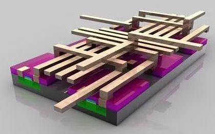
The surface of the chip appears exceptionally smooth, but it may contain more than 20 layers of complex circuits. When magnified, an extremely intricate network of circuits can be seen, resembling a futuristic multilayer highway system.
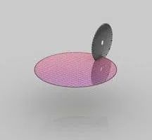
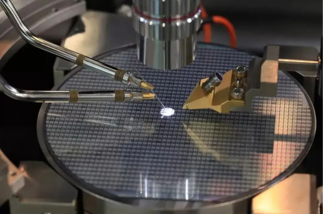
3
Wafer Testing
At the core level, approximately 10mm/0.5 inches. The image shows a portion of the wafer undergoing its first functional test, comparing it with the reference circuit pattern for each chip.
4
Wafer Slicing
At the wafer level, 300mm/12 inches. The wafer is sliced into pieces, each piece being a core (die) of a processor.
Stage Eight
1
Single Core
Core level. A single core cut from the wafer, shown here is the core of Core i7.
2
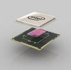
Packaging
At the packaging level, 20mm/1 inch. The substrate, core, and heat sink are stacked together to form the appearance of the processor we see. The substrate (green) serves as a base and provides electrical and mechanical interfaces for the processor core to interact with other parts of the PC system. The heat sink (silver) is responsible for dissipating heat from the core.
3
Removing Photo Resist
At this point, we have a complete processor (here is a Core i7).

Stage Nine

1
Grade Testing
The final test can identify the key characteristics of each processor, such as maximum frequency, power consumption, heat generation, etc., and determine the processor’s grade, whether it is suitable for the high-end Core i7-975 Extreme or the lower-end Core i7-920.

The above content describes the chip manufacturing process. We have now entered the technological era, heavily reliant on computer science and technology, with the CPU being an essential component of all computers. Not to mention the architectural design, the production of CPUs encapsulates the wisdom of humanity, employing the most advanced processes, production technologies, and cutting-edge machinery available in the world.
Material provided by: Xu Yiwen
Editor: Lan Wenping
Review: News Publicity Center
Source: Qingdao No. 67 Middle School , copyright belongs to the original author, please contact for deletion in case of infringement!
Global Physics
Global Physics focuses on physics learning and is committed to spreading physics culture. Specialized in physics, dedicated to physics! Aiming to stimulate learners’ interest in physics, sharing the wisdom of physics, and learning to think about problems with a physics mindset, presenting a fascinating, colorful, and magical physics.
Please contact [email protected] for submissions.