
Challenges in Chip Design

Challenges in Chip DesignSource: Synopsys Technology Zhihu, thank you!
Chips, as the core components of modern electronic products, have always played the role of the “brain”. They are extremely technology-intensive and capital-intensive, with production lines often costing tens to hundreds of billions of dollars.
The complete process of chip manufacturing includes several main stages: chip design, wafer manufacturing, packaging, testing, etc., each of which reflects technology and science.
For chips, both design and technology are complex. The birth of EDA technology in the 1980s—automated chip design—greatly reduced the difficulty of chip design and ultra-large-scale integrated circuits. Engineers only need to describe the chip’s functions using a chip design language and input it into a computer, which then compiles the language into a logic circuit using EDA tool software, followed by debugging. Just like editing documents requires Microsoft Office and image editing requires Photoshop, chip developers utilize EDA software platforms to design circuits, analyze performance, and generate chip circuit layouts. A modern chip contains hundreds of billions of transistors; without EDA tools, high-end chip design is simply impossible. Just think about how such a vast project could be completed manually!
The key point is that despite the advent of EDA, it does not mean that chip design is easy. Chip design remains a complex system engineering that integrates high precision and sophistication.
Challenges in Chip Design
Image from the internet, please delete if infringing.
Whether it’s IDM or fabless, the common characteristic is that chip design is at the core of the industry. For example, in 2018, AMD’s processors were outsourced to TSMC for manufacturing, using a 7nm process, while Intel’s processors still used a 14nm process, yet their performance still suppressed AMD, indicating that chip design is also crucial.
To design a chip, developers first need to clarify requirements, determine the chip’s “specifications”, and define key information such as instruction set, functions, input/output pins, performance, and power consumption, as well as divide the circuit into multiple small modules, clearly describing the requirements for each module.
Then, “front-end” developers design the “circuit” based on the function of each module, using computer languages to build models and verify their functionality. “Back-end” developers then design the “layout” based on the circuit, systematically imprinting billions of circuits onto a silicon wafer according to their connection relationships.
At this point, the chip design is considered complete. Such a complex design cannot have any defects; otherwise, it cannot be repaired and must be started from scratch. Redesigning and processing generally requires at least a year and an investment of tens of millions of dollars, sometimes even over a hundred million.
Pay attention! Since everyone generally has some understanding of the difficulty of chip manufacturing, this article hopes to help everyone have a common understanding of the challenges in chip design.

1

The First Challenge: Difficulty in Architecture Design
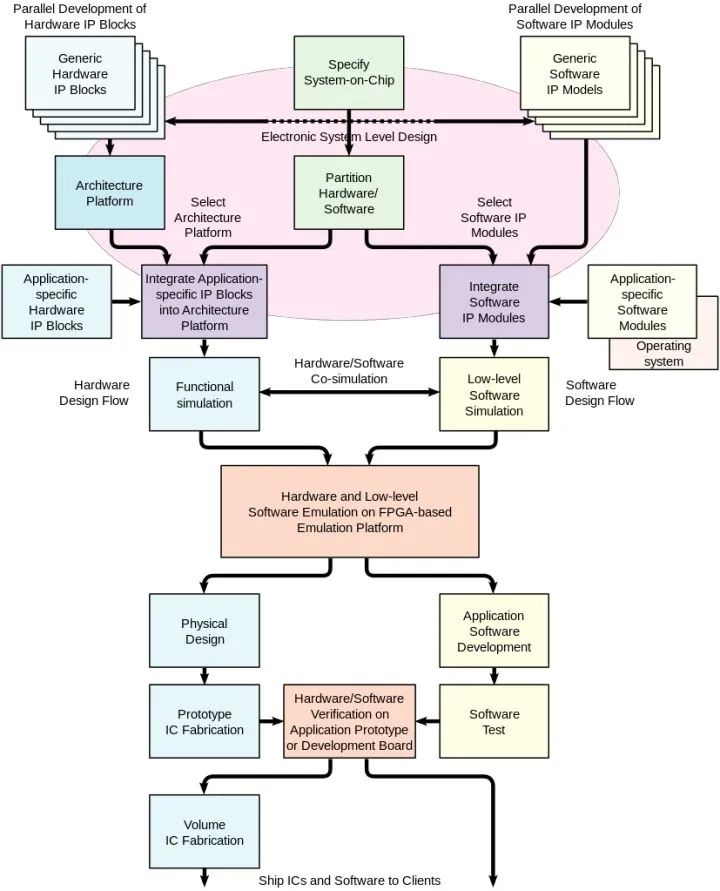
Chip design involves many stages, each facing numerous challenges. Taking the relatively simpler digital integrated circuit design as an example, it often adopts a top-down design approach, which includes:
Requirement Definition: Combining external environmental analysis, supply chain resources, and the company’s own positioning, propose the requirements for the next generation of products, further considering the product’s role, functions, required board quantity, and types of integrated circuits needed, precisely defining product requirements. The difficulty of this stage lies in accurately judging future trends in the market and technology, and having a full understanding of the capabilities of designers, manufacturing plants, and the entire industry chain.
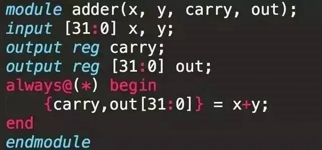
Function Implementation: Describing the goals that the chip needs to achieve, usually written in hardware description language. The difficulty here lies in grasping the overall performance and functionality that the chip can achieve, ensuring it meets the goals without exceeding its own capability limits.
Challenges in Chip Design
Image source from the internet, please delete if infringing.
Structural Design: Based on the characteristics of the chip, divide it into sub-modules with clear interfaces, well-defined relationships, and relatively independent functions. The difficulty of this stage lies in familiarity with the chip structure and whether it can meet requirements with as few modules and as low standards as possible.
Logic Synthesis: Developers convert the hardware description language into a logic circuit diagram. The difficulty here lies in ensuring the code is synthesizable, clear, concise, and readable, while sometimes also considering the reusability of modules.
Challenges in Chip Design
Image source from the internet, please delete if infringing.
Physical Implementation: Converting the logic circuit into a circuit diagram with physical connections. The difficulty lies in how to map from RTL description to synthesized library cells using as few components and connections as possible, achieving a gate-level netlist that meets area and timing requirements while ensuring internal interference-free.
Physical Layout: Delivering in GDSII file format to the wafer factory, creating the actual circuit on the silicon wafer, followed by packaging and testing to obtain the physical chip.
It must be noted that during chip design, many variables must be considered, such as signal interference and heat distribution. The physical characteristics of chips, such as magnetic fields and signal interference, vary greatly under different processes, and there are no mathematical formulas to directly calculate them, nor are there applicable empirical data to directly input. It can only rely on EDA tools to design step by step, simulating continuously and making trade-offs. After each simulation, if the results are unsatisfactory, it requires redesigning, which is a significant test of the team’s wisdom, energy, and patience.

2

The Second Challenge: Difficulty in Verification
The goal of chip verification is to iteratively validate through checks, simulations, and prototype platforms before chip manufacturing, to identify system hardware and software functional errors, optimize performance and power consumption, ensuring the design is precise, reliable, and meets the initially planned chip specifications.
Verification is not a process that occurs after design completion; it is a repetitive action that runs through every stage of the design, which can be subdivided into system-level verification, hardware logic functional verification, mixed-signal verification, software functional verification, physical layer verification, timing verification, etc.
Verification is challenging. First, verification can only falsify; it requires repeated consideration of potential problems and the use of formal verification methods to ensure the probability of correctness, which tests the experience and wisdom of designers.
Secondly, the methods for verification must be as efficient as possible. Modern chips integrate microprocessors, analog IP cores, digital IP cores, and memory (or external storage control interfaces), causing verification complexity to increase exponentially. How to complete increasingly complex verification quickly, accurately, comprehensively, and easily debuggable, entering the tape-out phase, is the greatest challenge for every chip designer.
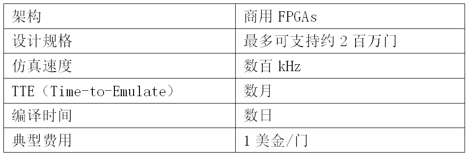
Finally, there are challenges with the verification tools themselves. Taking common FPGA hardware simulation verification as an example, in the 1990s, FPGA verification supported a maximum of 2 million gates, with each gate costing $1. Although the unit price has significantly decreased today, with the exponential growth in chip complexity, the number of gates for verification has risen to the scale of tens of millions and billions, making the overall costs even more staggering.
Challenges in Chip Design
Image source from the internet, please delete if infringing.
Moreover, FPGA itself is also a type of chip design. Now, large designs (greater than 20 million equivalent ASIC gates) require interconnection of multiple FPGAs for verification. The design of FPGAs faces practical requirements such as RTL logic segmentation, interconnection topology between multiple FPGAs, I/O allocation, layout, and observability, adding further difficulty to the design stage.

3

The Third Challenge: Difficulty in Tape-Out
Tape-out is trial production. After design completion, a chip foundry produces a small batch for testing. It may appear to be chip manufacturing, but it actually belongs to the chip design industry.
Tape-out is not technically difficult since chip design is based on existing processes. Apart from a small amount that requires guidance from chip design companies, the difficulty lies in money, money, and money.
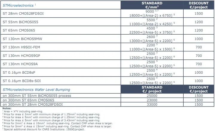
How expensive is tape-out? Let’s first quote the public pricing from CMP (Circuits Multi-Projets, a non-profit multi-project wafer service organization in the U.S.).
Challenges in Chip Design
Image from CMP pricing sheet
According to this quote, taking the industry’s smallest die area processor, Qualcomm Snapdragon 855 (size: 8.48mm × 8.64mm, area: 73.27 square mm), the standard price for tape-out using a 28nm process is €499,072.5, which is nearly 4 million RMB!
Then, what can chip design companies obtain? 25 bare chips, averaging 160,000 RMB each!
More importantly, tape-out is not a one-time event!
If tape-out fails, modifications are needed before retaping; if tape-out is successful, further modifications and optimizations may be required, followed by retaping.
Each time requires at least several million RMB.
What is meant by spending money? This is what it means to spend money!
Some may question why this cost issue is considered a difficulty. It is indeed a difficulty; the greatest difficulty in the world is lack of money, right?
The reason for mentioning tape-out costs is that many people point out that establishing an advanced process chip production line requires massive capital investment, but through tape-out, it becomes evident that chip design also has an astonishing thirst for funds.

4

The Fourth Challenge: Increasingly Challenging Design Requirements

Firstly, as chip usage scenarios extend to AI, cloud computing, smart cars, 5G, etc., the safety and reliability of chips have become more important than ever, imposing higher and stricter requirements on chip design.
Secondly, with the rapid development of AI and smart cars, there is a demand for dedicated chips and new architectures that adapt to industry needs, presenting more new challenges to chip design.
Lastly, as silicon-based chips reach the 1nm process limit in two to three years according to Moore’s Law, the responsibility of continuing to improve performance and reduce power consumption increasingly falls on chip design, adding greater pressure. Furthermore, advancements in process technology urgently require guidance from chip design to be realized, which adds additional pressure.
This Thursday (September 5th) at 16:00, E-course Network will invite an IC industry expert with over 15 years of experience to host a live broadcast filled with valuable insights!
This live open class will focus on career planning and development in the IC industry, introducing essential information about the chip industry, key positions, company distribution, career growth paths, and learning resources for newcomers who are about to enter or wish to enter the industry, aiming to help relevant university students enhance their industry awareness and arm themselves with knowledge and experience to prepare for future IC campus recruitment job hunting, ensuring they are well-equipped!
Students who want to obtain high-paying offers of 400K+ should not miss it~
For event details, please check the poster below, scan the code, and reply “Open Class” to register for free and join the group!

Challenges in Chip Design

Challenges in Chip Design

E-course Network (www.eecourse.com) is a professional integrated circuit education platform under Moore Elite, dedicated to cultivating high-quality integrated circuit professionals in the semiconductor industry. The platform provides a training environment that aligns with corporate needs, offering a comprehensive curriculum and practical training through both online and offline methods, rapidly developing students to meet corporate demands.

Founded in 2015, E-course Network has a mature training platform, a complete course system, and a strong faculty. It plans to establish a premium semiconductor course system with 168 courses, covering the entire integrated circuit industry chain, and has 7 offline training bases. E-course Network has a total of 517,000 fans, directly supplying 8,127 professionals to the industry. It has established deep cooperative relationships with 85 universities and has held 240 corporate training sessions.

Leave a Comment