What Is 7nm in Chip Technology?

What Is 7nm in Chip Technology?
Source: Semiconductor Research
Author: Guan Jian JamesG

Introduction

The 7nm process technology for chips is something we often hear about, but does 7nm really mean that the size of the chip is only 7nm? Let’s take a look!
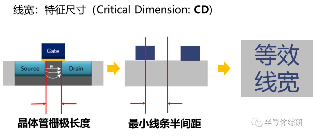
The image below is a classic cross-section diagram of a logic chip that I found online. From the diagram, you can see that the structure of semiconductor chips/devices is very complex, consisting of many layers stacked together:
The bottom layer, FOEL (Front End of Line), is the transistor structure part.
The layer above it, BOEL (Back End of Line), consists of metal lines (mainly copper) connecting the various transistors.
The topmost part is where the signal and power pins are brought out. This part is usually not processed at the wafer fab but at the packaging plant.
What Is 7nm in Chip Technology?
The structure of transistors/MOSFETs is also changing. Generally speaking, up to 28nm, the transistor structure is still the planar structure shown in the image below. Starting from 20nm, transistors have entered the era of 3D structures, the most typical being the FinFET structure shown in the image below. The confusion regarding the concept of transistor linewidth also starts from here.
What Is 7nm in Chip Technology?
Generally speaking, the term linewidth in the industry is referred to as CD/Critical Dimension, which directly translates to feature size in Chinese. It refers to the minimum width of lines in the chip structure, usually the length of the gate (as seen in the leftmost part of the image below).
Later, the length of the gate was no longer the minimum linewidth and could not accurately represent the process node. Thus, the industry began to use the minimum line width half-pitch to represent linewidth, which is half the distance between the centers of the two closest adjacent lines in all patterns. This value represents the highest graphic resolution in the chip structure.
The resolution in the technical parameters of lithography machines actually refers to this minimum line half-pitch (see the middle part of the image below).
However, with the advent of the FinFET process era, limited by the technical capabilities of lithography machines, the actual graphic resolution we can achieve has not significantly improved. However, due to changes in the transistor structure, its actual density has indeed increased significantly. So how should we evaluate the level of this technology?
Thus, wafer fabs came up with the concept of equivalent linewidth.
What Is 7nm in Chip Technology?
The image below shows the standard method for calculating transistor density published in Intel’s technical documentation. In simple terms, it calculates the transistor density using the area of a standard NAND gate (which contains 4 transistors) and then calculates the average transistor density using a standard Flip-Flop trigger circuit (which contains 6 NAND gates). The two density results are then weighted to obtain how many transistors can be made per unit area on the wafer under the current process technology.
This density value is then compared with the density of planar transistors to calculate the equivalent linewidth value. Therefore, even though we cannot significantly reduce the actual graphic linewidth, we can achieve an equivalent “small linewidth” by changing the device structure to reduce the area and increase density.
From the 20nm FinFET process onward, the so-called linewidth we see is all like this.
What Is 7nm in Chip Technology?
Of course, due to the use of equivalent conversion methods, this provides opportunities for various wafer fabs to take advantage of the situation. By exploiting loopholes in algorithms, the actual transistor density of chips with the same process node can vary significantly, and the differences can be quite large.
As seen in the image below: although both are called 10nm nodes, Intel achieved a transistor density of 106 million/mm², while TSMC and Samsung only achieved 53 and 52 million/mm², almost a difference of half.
The same situation persists in the subsequent 7nm and 5nm nodes. It is evident that in terms of naming, the honest Intel suffered a significant disadvantage, being bullied by the other two companies.
What Is 7nm in Chip Technology?
Since the naming of process nodes is unreliable, what methods does the industry use to measure the level of a specific process?
In fact, there are many indicators used to judge specific process technology in the FinFET process, but in most cases, it is enough to remember and understand two terms:
1) CPP: Contacted Poly Pitch, the distance between the polysilicon gates of the contact holes.
2) MxP: Metal Pitch, the distance between metal lines (usually referring to the distance between the first or second layer of metal lines).
CPP reflects the width of the entire transistor cell, while MxP is used to measure the height of the transistor cell, usually referred to as Track. The height of the transistor is a few times MxP, which is referred to as several Tracks or several Ts.
These two indicators represent the size of the transistors, which determines the density per unit area of the transistors. The image below is a reference:
What Is 7nm in Chip Technology?
Additionally, there is an indicator called Fin Pitch, and the ratio of MxP to Fin Pitch is referred to as Gear Rate.
Well, by now you should have a general understanding of linewidth in advanced processes.
This content is reprinted and represents only the author’s views.
It does not represent the position of the Semiconductor Institute of the Chinese Academy of Sciences.
Editor: Yu Ting
Editor-in-chief: Jiang Yu
Submission Email: [email protected]

What Is 7nm in Chip Technology?

Leave a Comment