Source: LightSense Technology
Original Author: BENG
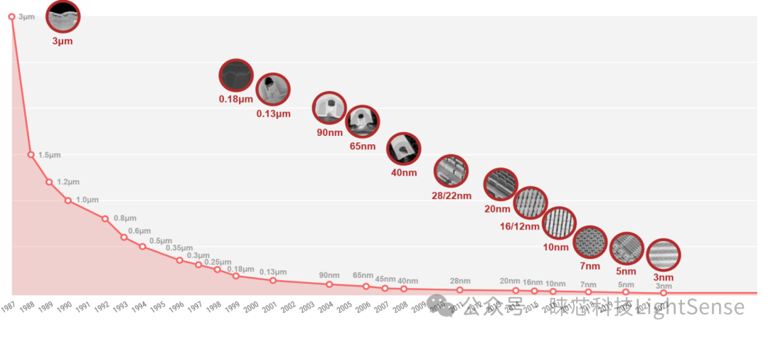
Different types of chips are accompanied by different node technologies. Except for logic chips, there is basically no need for technology smaller than 28nm.
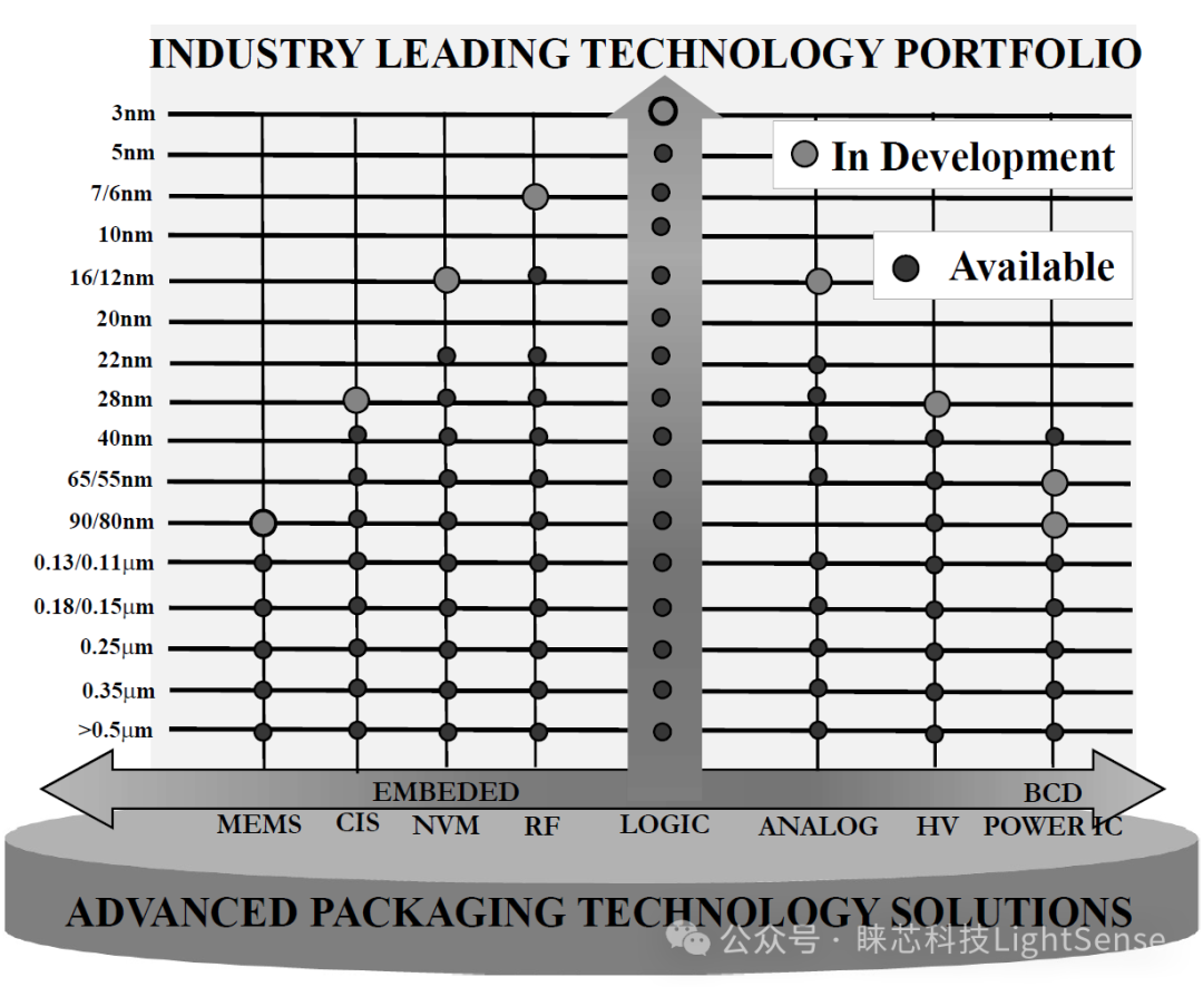
MEMS: Micro Electro Mechanical Systems (MEMS). Integrates industry-leading Complementary Metal-Oxide-Semiconductor (CMOS) and wafer stacking technology to manufacture monolithic micro-electromechanical systems (MEMS). TSMC’s sensor SoC technology ranges from 0.5 microns (µm) to 0.11 microns, supporting applications such as G-sensors, gyroscopes, barometers, microfluidics, and bio-gene chips.
CIS: CIS technology has completed the evolution from Front-Side Illumination (FSI) to Back-Side Illumination (BSI) and then to multi-wafer stacking. It has achieved 200 million pixels (200MP) mobile cameras, full-color night vision security/IoT cameras, 140db high dynamic range (HDR) automotive cameras, and 3-safety-stacked voltage domain global shutter (VDGS) augmented reality (AR)/virtual reality (VR) cameras. TSMC also continues to migrate stacked image signal processors (ISP) to achieve 12nm FinFET compact (12FFC) ISP, making CIS chips smaller, smarter, and more energy-efficient.
NVM: Non-Volatile Memory, including industrial standard one-time programmable memory (OTP), multi-time programmable memory, flash memory, and next-generation Magnetic RAM (MRAM) and Resistive RAM (RRAM) NVM.
RF: Radio Frequency. TSMC provides the industry’s most advanced and comprehensive Mixed Signal/RF CMOS (MS/RF) technology portfolio, selectable from 0.5µm to 4nm. It continues to launch innovations supporting various communication applications, including 4G/5G cellular systems, WiFi, and Bluetooth.
LOGIC: Logic chips.
ANALOG: Analog processing technology/analog chips serve as a communication interface between the real world and digital systems, accurately converting natural analog biological features, light, heat, speed, pressure, temperature, and sound into digital signals.
HV: High Voltage chips. TSMC’s high-voltage process ranges from 0.5 microns (μm) to 40 nanometers, providing higher quality panel driver images and lower application power consumption, including televisions, smartphones, tablets, smartwatches, and other portable electronic products.
BCD: Bipolar-CMOS-DMOS. TSMC’s BCD power management process features higher integration, smaller footprint, and lower power consumption, covering nodes from 0.6µm to 40nm, used in consumer electronics, communication devices, and computers.
POWER IC: Power chips.
END
The reproduced content only represents the author’s views.
It does not represent the position of the Institute of Semiconductors, Chinese Academy of Sciences.
Editor: Schrödinger’s Cat
Editor-in-Chief: Six Dollar Fish
Submission Email: [email protected]