In the PCB design process, layout is a key factor that determines circuit performance, manufacturability, and aesthetics. Mastering the layout operation commands and shortcuts in Altium Designer can significantly enhance work efficiency, allowing you to handle complex circuit boards with ease.
🛠️ 1. Basic Component Operations
This is the most frequent operation in layout, and mastering them is the first step.
- • Move Components
- • Operation: Move the cursor over the target component, hold down the left mouse button, and you can start dragging. This also applies to moving multiple selected objects.
- • Shortcut Operation:
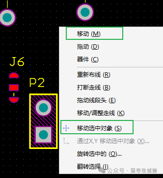
- • M, M: Execute the “Move” command. The most commonly used!No need to select beforehand, press M twice in succession (accelerated key usage).
- • M, S: Execute the “Move Selected Objects” command. Requiresprior selection of components before operation.
Insert image description here - • Rotate Components
- • Operation: While moving components, press the spacebar (Space) to rotate 90 degrees counterclockwise.
- • Note: This is an operation during the moving process, not a standalone command.
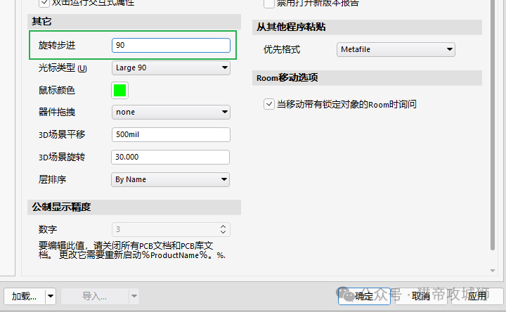
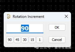
- • Tip: You can set the default rotation angle (e.g., 45 degrees) in the system parameters -> PCB Editor -> General, but 90 degrees is the most commonly used. If you need to frequently change the rotation angle, it is recommended to use scripts for quick operations.
- • Flip (Mirror) Components
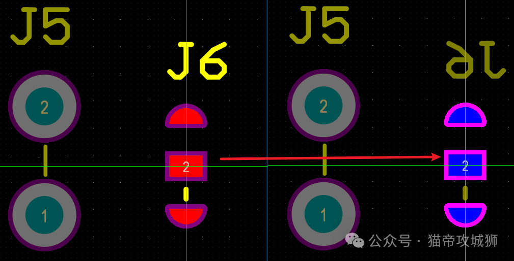
- • Operation: While moving components, pressL key to flip the component from the top layer (Top Layer) to the bottom layer (Bottom Layer), or vice versa.
- • Note: Similarly, you must pressL while in the moving state.
- • Tip: After flipping, the pads of the component will automatically switch to the corresponding layer, and the silkscreen will also be mirrored. You can use the left mouse button to long-press for in-place flipping, entering the moving state and pressingL to do so.
In-place flipping - • Align Components
- • Operation: Select two or more components that need to be aligned, right-click -> Align -> Choose alignment method (left, right, top, bottom, center horizontally, center vertically, etc.).
- • Shortcut: Shift+Ctrl+ (Left L, Right R, Up T, Down B, etc.).
- • Tip: Alignment is key to achieving a professional and tidy layout.
- • Equidistant Distribution
- • Operation: Select three or more components, right-click -> Align -> Vertical/Horizontal Distribution. Ensure that there is a “boundary” component among the selected components for reference.
- • Shortcut: Shift+Ctrl+ (Horizontal H, Vertical V, etc.).
- • Tip: Used to create evenly spaced arrays, such as buttons, LEDs, etc.
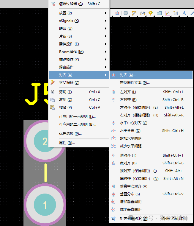
Component alignment operation
⚙️ 2. Common Operation Shortcuts and Accelerated Keys in Altium Designer PCB Layout
The following lists the most practical operation commands and shortcuts during the PCB layout phase to help you complete your design work faster.
| Shortcut | Function Description |
| Shift+Ctrl+X | Open or close cross-selection mode |
| Ctrl+H | Select all electrical objects connected to the same net (useful for finding connected components). |
| Shift+F | Find similar objects |
| Shift+C | Clear filters (useful for clearing selection states) |
| Shift+S | Cycle through single-layer mode |
| Shift+Ctrl+L | Align selected objects by left edge |
| Shift+Ctrl+R | Align selected objects by right edge |
| Shift+Ctrl+H | Equalize horizontal spacing of selected objects |
| Shift+Ctrl+V | Equalize vertical spacing of selected objects |
| Shift+Ctrl+T | Align selected objects by their top edge |
| Shift+Ctrl+B | Align selected objects by their bottom edge |
| Ctrl+End | Jump to the current origin |
| Ctrl+Shift+Scroll Wheel | Switch working layers |
| Ctrl+M | Measure distance |
| Space | Rotate selected objects while moving |
| F5 | Show/hide net colors |
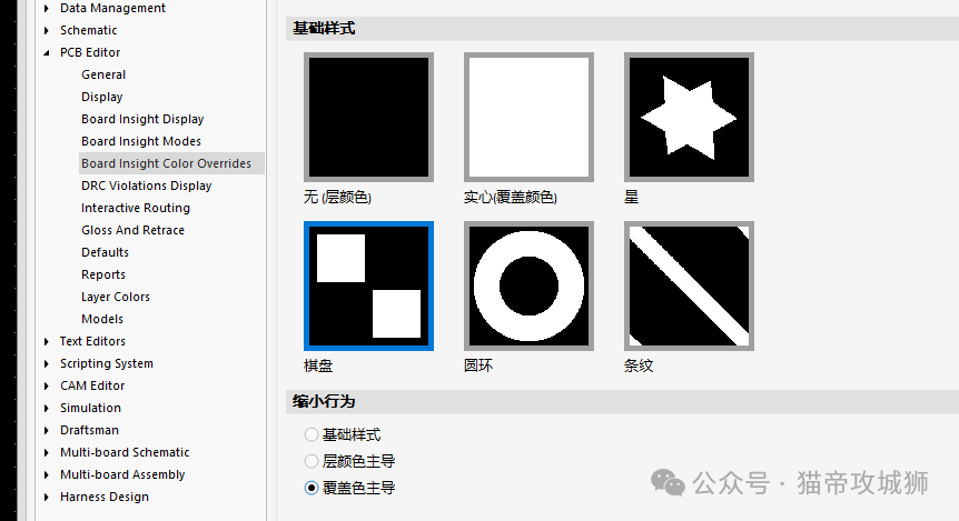
| Accelerated Keys | Function Description |
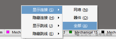
| N | Show/hide connection/net flying lines |
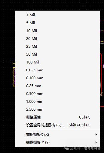
| G | Bring up the quick grid settings menu |
| T+C | Click on components in PCB, locate components in schematic (cross-selection mode must be enabled) |
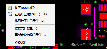
| T+O+R | Arrange components according to ROOM |
| T+O+L | Arrange within a rectangular area (perform after selecting components, schematic selected, PCB quickly categorized) |
| I+L | Arrange within a rectangular area (perform after selecting components, schematic selected, PCB quickly categorized) |
| M+M | Move objects |
| J+C | Jump to component |
| D+S+D | Define board shape according to selected closed curve |
| L | View configuration (set component display, transparency, etc.), the new version can set to always display a certain layer |
| J+C | Jump to component |
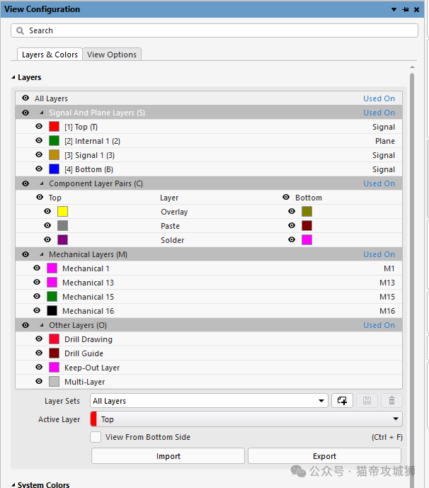
🚀 3. Conclusion
By mastering these shortcuts and operation commands, PCB layout efficiency can be quickly improved. If there are any operations or shortcuts not mentioned that are used during layout, feel free to leave a comment to supplement.
————>> THE END <<————


 Please like and follow
Disclaimer
The content published by this public account, including technical articles, circuit designs, code examples, etc., is for the purpose of information exchange and technical learning. All content is for reference only and does not guarantee its accuracy or applicability. Readers should verify technical solutions themselves and assume corresponding risks. The author and the public account do not bear legal responsibility for any losses caused by the use of this content.
In addition, the third-party products, tools, or technology names mentioned in the text are owned by their respective companies, and the references are for illustrative purposes only, not representing any commercial recommendation or partnership.