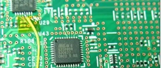
In the PCB design community, there is an “invisible hero” that is often overlooked by beginners — it may seem like an inconspicuous little dot, but it can transform a product from “frequent rework” to “one-time success,” and from “cost overruns” to “efficient mass production.”
This is the Mark point. Today, let’s discuss in simple terms why it is essential to place Mark points in PCB design and how to do it correctly to avoid pitfalls.
Don’t Underestimate This Little Dot! 5 Major Functions, Missing One Can Be Troublesome
Some may ask: “If the PCB traces I designed are correct, is it necessary to place this point?” The answer is no! Although the Mark point seems simple, it is actually a “navigator” that runs through PCB manufacturing and assembly. Without it, the subsequent processes can become chaotic.
1. Ensures Component Placement with “Zero Deviation,” Bidding Farewell to “Hectic Operations”
Currently, mainstream SMT (Surface Mount Technology) relies on machines to automatically place components onto the PCB. But how does the machine know “where to place the component”? The answer is the Mark point.
By recognizing the Mark point, the machine can accurately locate the position and angle of the PCB. Even if the PCB is slightly misaligned, it can automatically adjust. Without the Mark point, either manual alignment is required (which is painfully slow), or the machine may place components incorrectly, resulting in product scrap.
Even in scenarios requiring manual assembly, the Mark point helps operators quickly find the correct position, which is much more convenient than measuring against a drawing.
2. Shortens Manufacturing Cycle, Doubles Efficiency
The first step in PCB manufacturing is to determine the position of the board. In the past, without Mark points, workers had to manually measure and mark using a ruler. This was manageable for a single board, but during mass production, just positioning could take a lot of time.
With Mark points, it’s different — machines can instantly “grab” the markers, completing positioning in seconds, significantly reducing preparation time. This boosts production efficiency and allows for faster product delivery, which is a real competitive advantage.
3. Reduces Rework Waste, Directly Lowers Costs
Human operations are prone to errors: for example, misplacing components or misaligning the board during soldering… These mistakes can lead to PCB scrap, and re-manufacturing not only costs money but also delays timelines.
The Mark point allows for more precise automated operations, reducing the chances of “misplacing or mis-soldering” from the source. Don’t underestimate this; in mass production, reducing scrap by just 10% can save a significant amount of costs.
4. Prevents Reflow Soldering Failures, Significantly Reduces Defect Rates
After components are placed on the PCB, they must go into a reflow oven for heating, allowing the solder to melt and secure the components. This process has very high alignment requirements — if the board is not positioned correctly, components may shift during heating, leading to cold solder joints.
With Mark points, the reflow soldering machine can automatically align the PCB, ensuring that the heating position and time for each board are precisely consistent, which directly reduces defect rates, eliminating the need to spend time sorting and repairing faulty boards.
5. Ensures Product Stability, Providing Greater Peace of Mind
Whether it’s a smartphone, computer, or industrial equipment, the stability of the PCB directly determines the product’s lifespan. Mark points ensure that every PCB’s manufacturing and assembly are “standardized” — there won’t be some boards with components placed correctly and others misaligned.
With increased consistency, the stability and reliability of the product naturally improve, significantly reducing the probability of subsequent failures.
How to Place Mark Points? 3 Key Details, Even Beginners Can Get It Right the First Time
Now that you understand the importance of Mark points, the next step is to know “how to place them correctly.” The method is quite simple; just remember these 3 key points:
1. Style & Size: Follow the “1-2-3” Standard, Don’t Make Your Own Changes
Mark points are not just random circles; they have a fixed “golden ratio”:
- The center is a 1mm diameter pad (equivalent to the core of a small circle);
- Surrounding it is a 2mm diameter solder mask opening (to expose the pad for easy machine recognition);
- The outermost layer is a 3mm diameter lead (which can be circular or polygonal, depending on personal preference, no difference).
Just stick to these dimensions; there’s no need to innovate — after all, factory machines are calibrated to this standard, and changing it may lead to recognition issues.
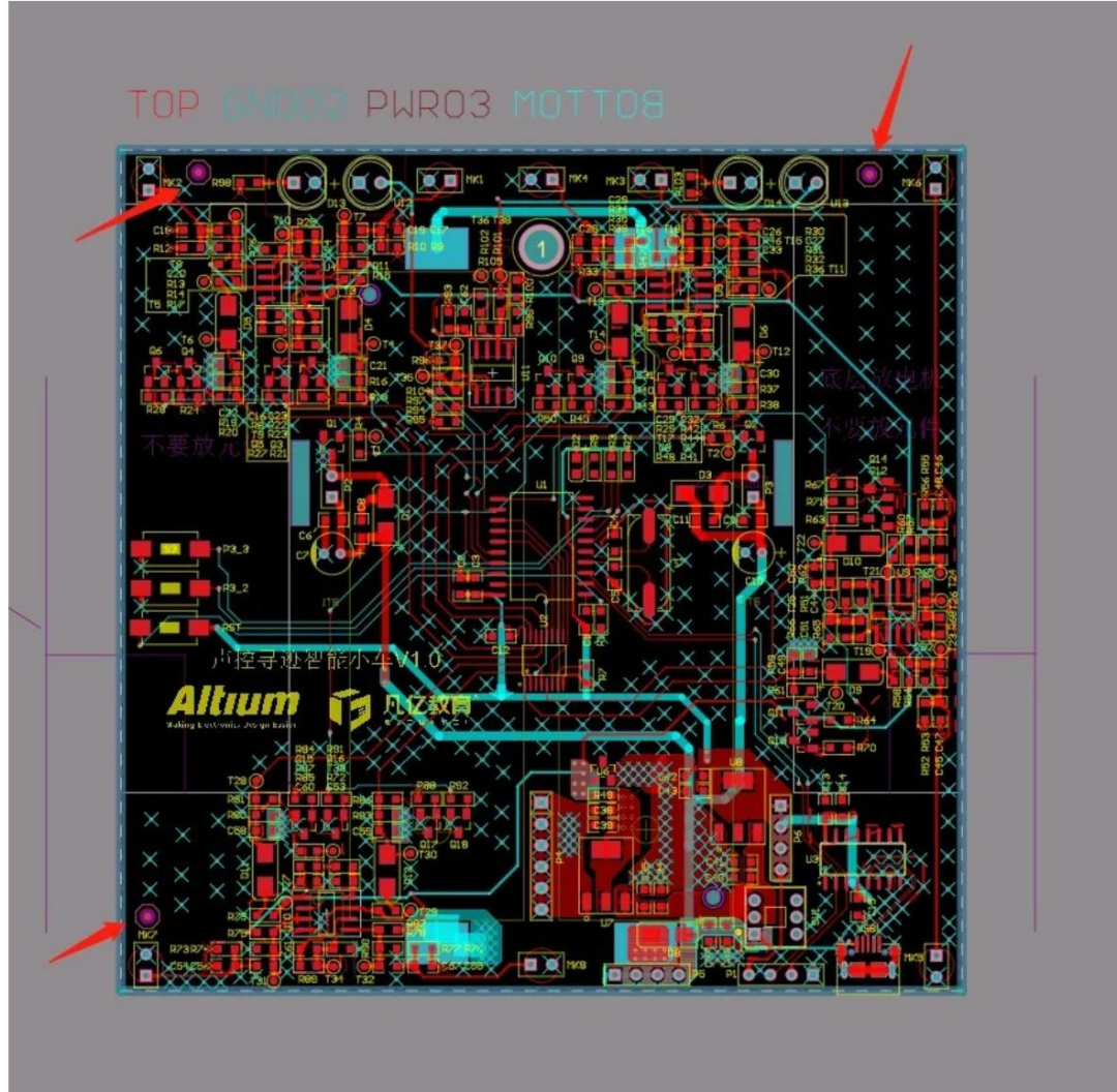
2. Position: Prioritize the “Component Side,” 3 Points Are Enough
- Where to place: If the PCB has components on only one side (single-sided layout), place it only on that side; if both sides have components, place it on both sides.
- How many to place: 3 points on one side are sufficient; more would be redundant.
- Specific position: It’s best to place them in the corners near the edge of the board, about 3mm away from the edge — this allows for easy machine recognition without affecting the layout of other components.
Final Reminder: Don’t Wait Until Errors Occur to Remember It!
Many beginners focus on the circuit and layout when designing PCBs, only to forget to place Mark points. When the factory reports “unable to produce” or “placement errors,” they then go back to make modifications, which not only wastes time but may also delay the project.
In fact, designing Mark points is not complicated; spending a few minutes to place them according to standards can save countless troubles later. Remember: the “last mile” of PCB design often hides in these seemingly inconspicuous small details.
Have you ever encountered pitfalls with Mark points while designing PCBs? Feel free to share your experiences in the comments, and don’t forget to forward this to friends who need it, so we can all avoid pitfalls together!
 Note:This article is an original piece by Fan Yi Education, please indicate the source when reprinting!For submissions/recruitment/advertising/course collaboration/resource exchange, please add WeChat: 13237418207
[Practical Tips] How to Handle Inductors for More Stable PCBs! Lower EMI!
2025-07-23
When Do PCBs Need Mechanical Cutting?
2025-07-23
How to Properly Copper Pour in High-Speed PCBs? 99% of Engineers Overlook These Points!
2025-07-21
The Role of PCB Jumpers and Correct Usage Techniques, 90% of Engineers Overlook!
2025-07-17