1
Introduction
Throughout the entire product lifecycle, PCBA design plays a crucial role in the product’s performance, quality, and cost control. Generally, design costs account for about 8% of the total product cost, yet they determine approximately 80% of the total product cost, with about 80% of design deficiencies or errors only being discovered during the manufacturing and usage processes.
If an error is identified and corrected during the design phase, the cost may be 10, whereas in the production phase, it could escalate to 100, directly leading to an extended product launch cycle.
With the rapid advancement of science and technology, the structure and functionality of modern electronic products are becoming increasingly complex. Under the premise of ensuring product functionality, performance, quality, and reliability requirements, how to reduce manufacturing costs and shorten product production cycles is key to market competition.
Most quality issues in product manufacturing are caused by design; implementing manufacturability design and assembly reliability design aims to eliminate problems as much as possible during the design phase, thereby shortening the product design cycle and improving product design quality.

1. Component Manufacturability Selection – The Foundation of PCBA Manufacturability Design
1. Basic Principles for Component Selection
1.1 Component selection should meet specific customer requirements, design requirements, appropriate electrical performance, reliability, and usage requirements, and align with the assembly and testing capabilities of the enterprise.
1.2 Components should have a price advantage and no supply issues.
1.3 Dimensions and shapes should be standardized, with good dimensional accuracy and interchangeability.
1.4 When selecting components, consider the processing technology to simplify the process and reduce processing costs.
a) Prioritize the selection of SMT components that can be automatically assembled. The center upper surface of SMT components should be flat;
Note: This facilitates the vacuum nozzle of the placement machine to pick them up.
b) Avoid selecting irregular components and manual insertion components as much as possible, and reduce the use of through-hole insertion components and manual insertion components;
Note: Costs are higher than those of automatic insertion components.
c) Avoid SMT/PTH mixed assembly as much as possible, especially avoid installing PTH components on both sides of the PCB;
Note: This leads to some PTH components being only manually assembled, increasing costs and reducing quality.
d) Aim to distribute components evenly across the PCB;
Note: This reduces warping and helps with uniform heat distribution during soldering.
1.5 SMT components should have a certain mechanical strength to withstand the placement stress from the placement machine and the bending stress of the substrate.
Note: This is to prevent damage to components and solder joints during soldering and assembly.
1.6 Avoid using a mix of leaded and lead-free components in the same product.
Note: This meets the reliability and environmental requirements for soldering.
1.7 Terminals and pins should comply with IPC/EIA J-STD-002 “Solderability Tests for Component Leads, Terminals, and Solder Pads”.
Note: This ensures 95% solder coverage.
1.8 The PCB should meet the solderability requirements of J-STD-003 “Solderability Tests for Printed Circuit Boards” or equivalent documents.
Note: This ensures 95% solder coverage.
1.9 Components should be able to withstand reflow and wave soldering temperatures according to IPC/JEDEC-J-STD-020 “Moisture/Reflow Sensitivity Classification for Non-Hermetic Solid State Surface Mount Devices” requirements, capable of withstanding 2-3 cycles, and all components should endure the process temperature.
Note: To ensure soldering repeatability, clear constraints should be established for soldering parameters such as maximum temperature rise rate, cooling rate, high-temperature dwell time, maximum component body temperature, and PCB surface temperature during wave soldering.
1.10 Meet complete MSD specifications.
Note: MSL is clearly marked on the component label, and handling, packaging, transportation, and usage should follow IPC/JEDEC-J-STD-033 “Handling, Packing, Shipping and Use of Moisture/Reflow Sensitive Devices” requirements.
1.11 Meet electrostatic discharge (ESD) requirements. Minimum electrostatic voltage.
Note: Manufacturers should implement ESD control programs according to ANSI/ESD IEC 61340-5-1, MIL-STD-1686, or agreements between users and suppliers.
1.12 Minimize the use of components smaller than 0402, larger than 1812, MELF components, and other components requiring special handling.
Note: The installation of irregular components requires manual operation or specialized equipment, resulting in poor assemblability and testability, increasing manufacturing costs.
1.13 Irregular components such as connectors and switches should be designed to be flame-retardant and high-temperature resistant.
Note: This avoids thermal deformation and cracking, withstanding soldering temperatures of up to 270°C.
1.14 If the product requires cleaning, components should be able to withstand water cleaning processes.
Note: The component packaging must meet airtightness requirements to avoid compromising reliability after assembly.
2. Verification Requirements for New Package Components
At the design stage, for new or complex package types such as SIP, CSP, BGA, QFN, MCM, if these components are new to the enterprise, appropriate verification must be conducted before use, considering the following factors:
2.1 Tools: such as stencil and carrier design, reflow soldering requirements, etc.
2.2 Process control: such as printing parameters, wave soldering parameters, crimping force settings, soldering temperature curves, rework requirements, etc.
2.3 Assembly reliability: the integrity of mechanical interconnections between components and printed circuit boards, such as solder joints, crimped assemblies, etc.
2.4 When components require verification, please request the component supplier to provide test reports based on the following standards.
1) Solderability testing: according to IPC/EIA J-STD-002 “Solderability Tests for Component Leads, Terminals, and Solder Pads”;
2) Solder joint reliability testing: according to IPC-9701 “Performance Test Methods and Qualification Requirements for Surface Mount Solder Joints”;
3) Mechanical shock and vibration: refer to MIL-STD 833 “Microelectronic Device Test Methods and Procedures”;
4) High-temperature storage: according to JESD22-A103 “High-Temperature Storage Life”; 5) Lead-free components also require simulation testing for tin whisker growth;
Note: Testing for tin whisker growth should be conducted on pure tin plating and tin plating with a purity greater than 95%.
6) Moisture-sensitive component level determination, refer to IPC/JEDEC J-STD-020 standard.
Note: Preferably select moisture-sensitive components with MSL below MSL4 for easier assembly, storage, and control.
7) Maximum package size withstand reflow soldering temperature.
Note: Generally, the maximum size component should not be lower than 250°C, refer to “IPC/JEDEC J-STD-020” Table 4-1.
8) Components should also consider compatibility with auxiliary materials in the assembly process.
Note: Such as compatibility of no-clean solder paste, water-soluble solder paste, wave soldering flux, conformal coatings, etc. with the components.
3. Components Not Recommended for Use
Avoid selecting the following components that are not recommended for use.
3.1 SMT components with a pitch less than 0.4mm (0.016in), BGA devices with solder ball diameters less than 0.25mm (0.010in).
Note: This can easily lead to bridging and cold solder joints.
3.2 SMT lead components with coplanarity greater than 0.10mm (0.004in).
Note: This can easily lead to insufficient solder or cold solder joints.
3.3 Packages smaller than 0201 in imperial size.
Note: This can easily lead to misalignment and tombstoning.
3.4 Using MELF components can result in lower product yield.
Note: Less solder area, difficult to place, misalignment, etc., leading to poor soldering reliability.
3.5 Components without polarity and manufacturer identification.
Note: This lacks foolproofing and can easily lead to installation errors.
3.6 Components that cannot be automatically placed or require special tools for placement and insertion.
Note: This increases costs and labor time, and results in poor soldering quality.
3.7 Components requiring special pre-processing techniques.
Note: Such as pin trimming and forming processes, increasing costs, labor time, and the probability of damaging components.
3.8 Components with high mounting heights.
Note: This can affect the normal transport of PCBs on the conveyor belt, especially important during mass production; the maximum component height is related to the brand of the placement equipment.
4. Components Meet RoHS Requirements (Including Component Packaging Body, Terminal and Pin Materials, Coatings, etc.)
4.1 Definition: RoHS is the “Directive on the Restriction of the Use of Certain Hazardous Substances in Electrical and Electronic Equipment”.
Note:
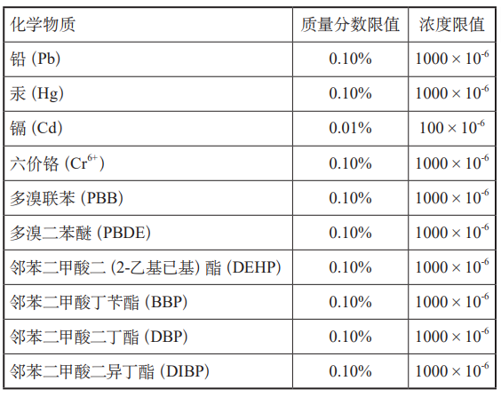
1) The RoHS 1.0 directive was released in 2003, requiring that electronic products placed on the EU market from July 1, 2006, must not contain harmful substances such as Pb, Hg, Cd, hexavalent Cr, polybrominated biphenyls (PBB), and polybrominated diphenyl ethers (PBDE).
2) RoHS 2.0 is an upgraded version of RoHS 1.0, which officially added four phthalates (DEHP, BBP, DBP, and DIBP) to the restricted substances list on June 4, 2015, with limits of less than or equal to 0.1%, implemented on July 23, 2019.
4.2 RoHS Compatibility
Note: Materials used in components and assembly (PCBs, components, solder metal materials, non-metal materials, chemicals, etc.) must meet all component requirements listed in the RoHS directive.
4.3 RoHS Exemptions
Note: The RoHS directive restricts the use of certain hazardous substances in electrical and electronic products and their components, but certain hazardous substances that are currently prohibited may be technically or scientifically infeasible, and these applications may be exempt from RoHS directive restrictions.
For example, high Pb solder with a lead content exceeding 85% is exempt due to its high melting point, particularly the 5Sn-95Pb solder with a melting point of 300 to 314°C.
The reasons for the exemption are:
1) The solder’s melting point reaches 300°C, which is particularly suitable for component packaging, as subsequent lead-free reflow and wave soldering temperatures are generally below 270°C, preventing the melting of the solder joints in the package;
2) Research results indicate that no suitable alternatives have been found in the field of lead-free solder.
Table 1: RoHS 2.0 Requirements for 10 Substance Content Standards
5. Requirements for Component Soldering Temperature Resistance
5.1 Surface mount components with lead soldering withstand 240°C, while lead-free soldering temperatures can reach up to 260°C, necessitating consideration of the thermal resistance of component packaging.
5.2 Components should be able to withstand the maximum allowable temperature without damage; the actual temperature distribution during production may be lower than this value.
5.3 A lower maximum peak temperature is acceptable for larger components (220°C for leaded, 245°C or 250°C for lead-free).
5.4 According to IPC-J-STD-020 standards, the temperature resistance requirements for component packaging during reflow soldering are shown in Table 2.
Table 2: Component Packaging Temperature Resistance for Reflow Soldering
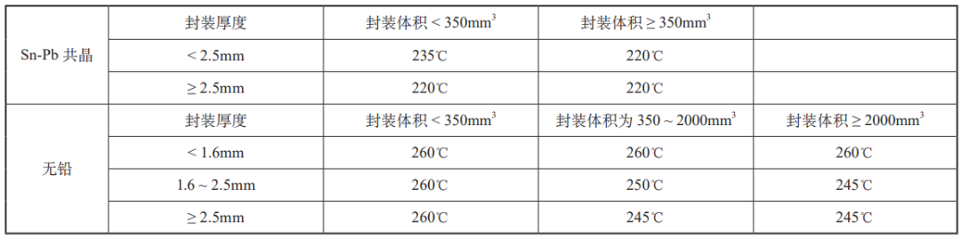
Note: For lead soldering, reflow soldering is at 235°C ±5°C for 10-15s; wave soldering is at 260°C ±5°C for 5s ±0.5s. For lead-free soldering, reflow soldering is at 260°C ±5°C for 10-15s; wave soldering is at 260°C ±5°C for 10s ±0.5s.
5.5 Different components have different temperature resistance modes.
Note:
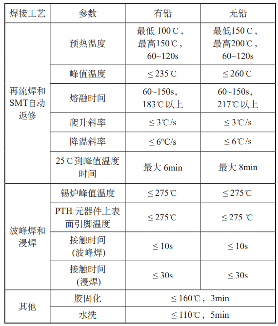
1) High-temperature resistant but not shock-resistant modes, such as ceramic capacitors, resistors, ferrite inductors, and glass diodes, can lead to cracks and breakage if the temperature rise or fall rate is too steep; refer to Table 3.
Table 3: PCBA Assembly Component Process Temperature Requirements
2) Shock-resistant but not high-temperature resistant, such as tantalum capacitors, aluminum electrolytic capacitors, and components with large thickness and package size that are not high-temperature resistant.
3) The temperature resistance curve of the three indicators of components: thermal shock resistance, i.e., temperature rise rate (°C/s), the maximum temperature the component can withstand, and the time it can endure at the maximum temperature; refer to Figure 1.
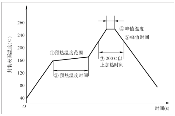
Figure 1: Component Packaging Temperature Resistance for Reflow Soldering
6. Requirements for Component Moisture Sensitivity
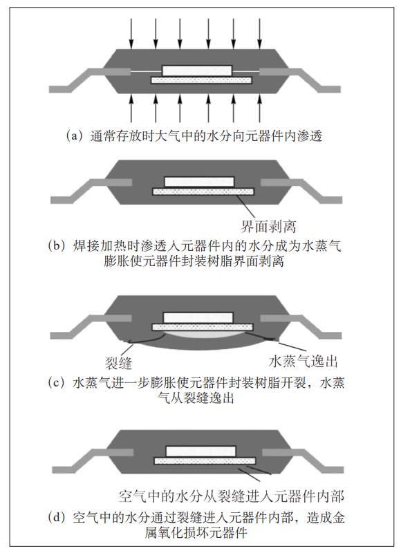
6.1 Definition of moisture-sensitive components and the mechanism of damage during high-temperature soldering.
Components absorb moisture, and during high-temperature soldering, MSD may be exposed to temperatures exceeding 200°C. During high-temperature soldering, moisture within the components evaporates, generating vapor pressure that can rupture the components, damaging their performance, potentially causing internal silicon chips or gold wires to break or delaminate. In severe cases, this can lead to the “popcorn effect,” as shown in Figure 2.
Figure 2: Mechanism of Damage to Moisture-Damaged Components
6.2 Packaging Requirements for Moisture-Sensitive Components
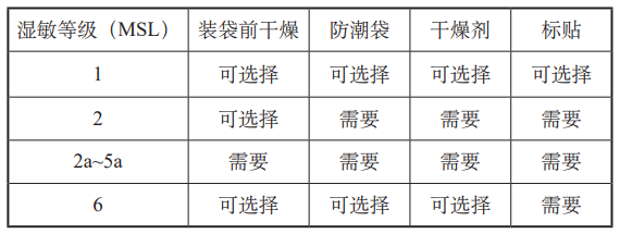
Common MSDs, such as plastic-packaged components and PCBs, are delivered in moisture barrier bags (MBB) that are vacuum-sealed, with desiccants and humidity indicator cards (HIC) inside. Incoming inspection should verify the integrity of the packaging and the color change of the HIC, as shown in Figure 3 and Table 4.
Figure 3: HIC Requirements
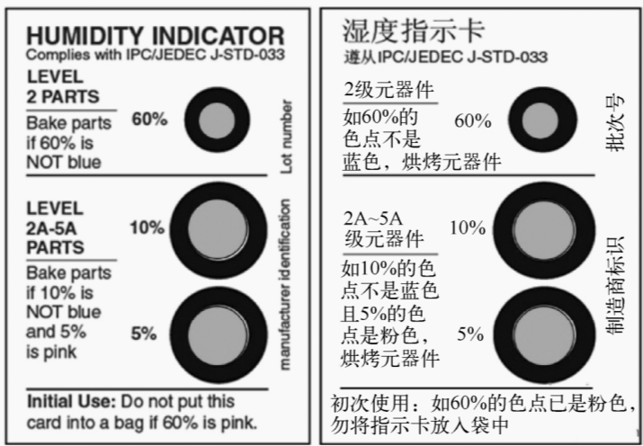
Table 4: Packaging Requirements for Moisture-Sensitive Components
The HIC can be reused after baking, and it should be used only after the 5% scale has completely turned blue. It is recommended to bake the HIC at 125°C for 2 hours, and it should only be reused once.
Note: Common component packaging materials include plastic, metal, glass, and ceramics. Generally, all plastic packaging materials are non-hermetic, making moisture-sensitive MSD components susceptible to moisture.
6.3 Component Moisture Sensitivity Level, select components with moisture sensitivity levels below 4.
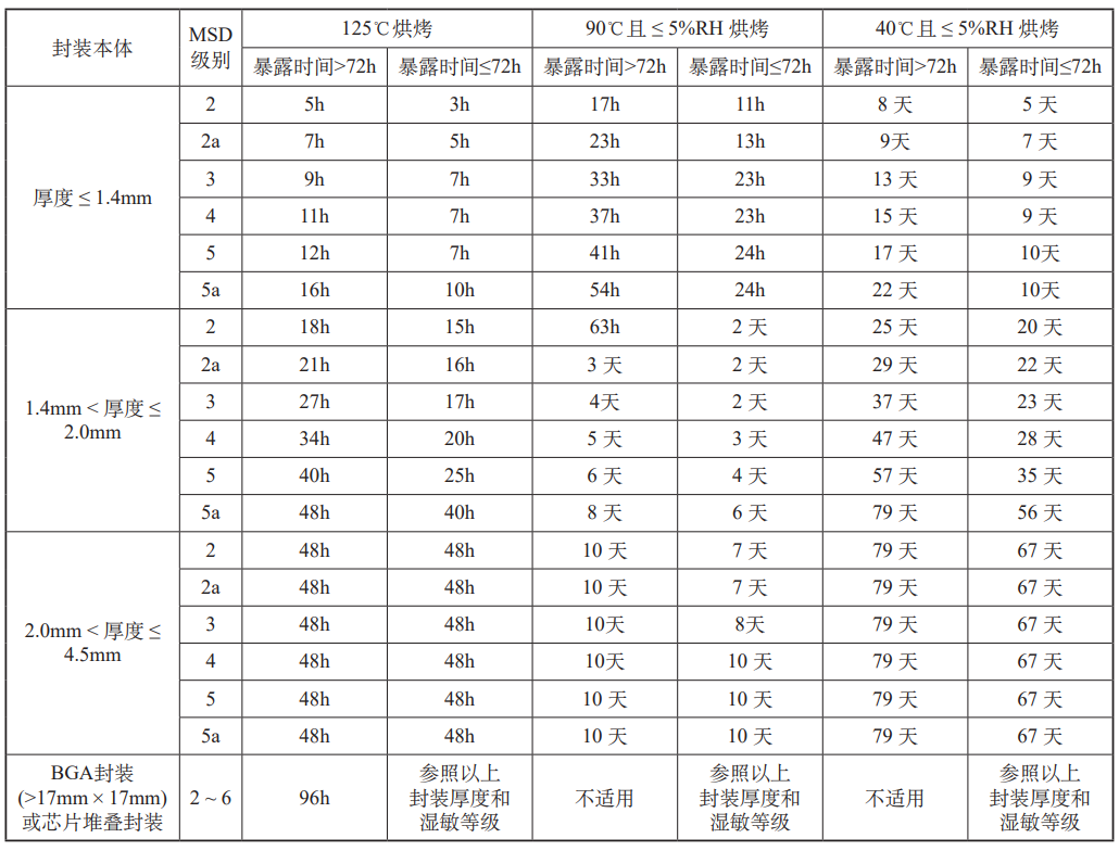
Moisture-sensitive component open life and baking requirements are shown in Tables 5 and 6.
Note: Preferably select components with low moisture sensitivity levels, as these components have relatively relaxed usage conditions and process controls; selecting components with high moisture sensitivity levels will increase manufacturing costs due to baking, short exposure time control cycles, and the need to optimize temperature curves.
Table 5: Open Life of Moisture-Sensitive Components
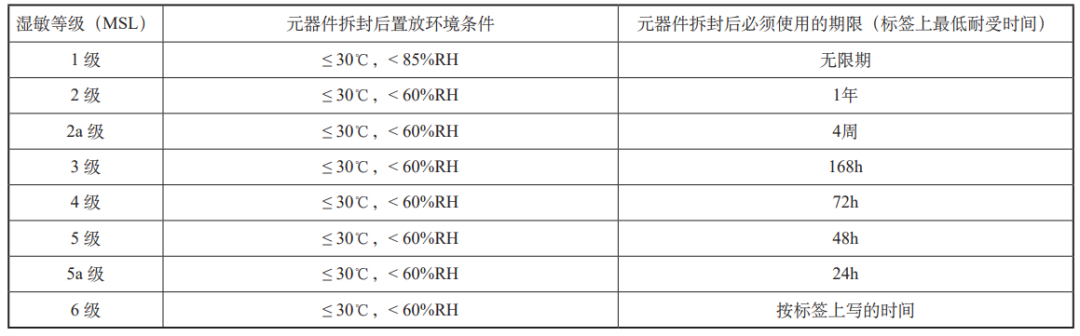
Table 6: Baking Conditions for Components
6.4 Control of Moisture-Sensitive Components
1) The control of MSD refers to the standard methods for handling, packaging, transporting, and using MSD materials of different moisture sensitivity levels.
Note: This is to avoid moisture damage that can lead to decreased product quality and reliability during high-temperature reflow. Refer to IPC-STD-033, IPC-STD-020.
Check for moisture barrier packaging (sealing date and shelf life, whether the moisture barrier bag is tightly sealed without openings or tears, whether there are MSD warning labels on the bag, and whether there are desiccants and humidity indicator cards (HIC) inside the packaging. During open sampling inspection, exposure time should be controlled within 30 minutes; if the HIC changes color, it must be baked or the supplier should be contacted for handling.
2) Determine if the MSD has absorbed moisture.
Note: If the storage time exceeds 12 months, exposure time exceeds the allowable usage time, the color on the HIC turns pink, or the status of the components cannot be tracked and determined, it indicates that moisture has been absorbed, requiring baking or recalculating the open life.
3) Baking precautions:
a) High-temperature baking should ensure that the packaging materials can withstand 125°C; generally, bake for 2-4 hours;
b) The number of baking times should be less than the maximum allowable baking times, which is 1-3 times at most (2a level components can be baked a maximum of 3 times, 3-5 level components can be baked a maximum of 2 times, and 5a level components can be baked a maximum of 1 time).
c) The baking temperature should be 125°C ±5°C, and the total baking time for multiple bakings should not exceed 48 hours; if the oven is opened midway, it should be ensured that it returns to the original set state within 1 hour.
4) Short-term exposure principles:
a) For components of levels 2-4, if the exposure time is less than 12 hours, they can be stored in a dry box with less than 5% RH, and the time should reach 5 times the exposure time, recalculating the MSD exposure time.
b) For components of levels 5 and 5a, if the exposure time is less than 8 hours, they can be stored in a dry box with less than 5% RH, and the time should reach 10 times the exposure time, recalculating the MSD exposure time. (To be continued)
[This article is adapted from “Step by Step New Technology” magazine, authored by Guo Hongfei, Senior Engineer of PCBA Reliability. Currently serves as the head of the PCBA Reliability Laboratory at Zhejiang Chint Electric Co., Ltd.]