Back drilling is a commonly used process technology in the manufacturing of printed circuit boards. It involves drilling out a portion of the via from either side to a predetermined depth, thereby shortening the total length of the via. The goal is to achieve more blind and buried via structures with the least number of lamination cycles while ensuring signal integrity or achieving circuit insulation.
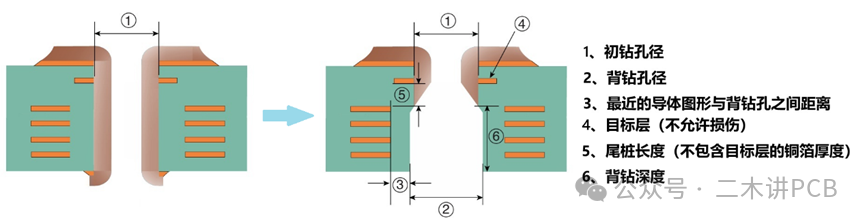
Figure1 Diagram of Back Drilling Structure
There is a special type of back drilling known as “shallow back drilling,” which not only removes the outermost (surface) metal but also drills away approximately0.05–0.127 mm of the wall metal, which is less than the thickness of a single dielectric layer. The purpose is to prevent any components directly above or below the via on the back drilling side from short-circuiting with the casing.
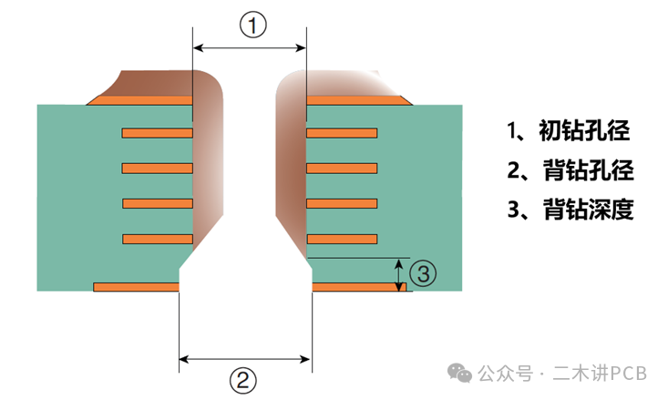
Figure2 Diagram of Shallow Back Drilling Structure
The inner or outer surfaces of back drilled holes must not contain any coating debris, loose particles (conductive or non-conductive), or residues from external connection pads. For standard digital circuits, there are no explicit restrictions on the tail length, as long as the on-off network relationship is correct. However, for high-speed and RF circuits, the tail length can significantly affect signal integrity, and it is generally required to be controlled within0~+0.15mm range.