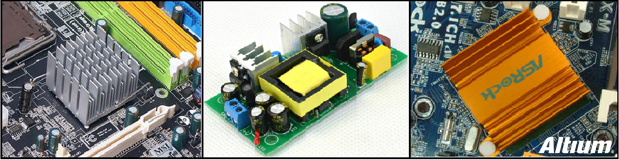
As electronic products continue to miniaturize, the heat dissipation requirements of these systems have increased as more functions are packed into smaller devices. This is especially true for PCBs operating under high current. Particularly, power systems with heavy loads, such as lithium-ion batteries used in electric vehicles, require integrated power management systems on the PCB. Additionally, high-current drive circuits must pay special attention to heat dissipation. Designers need to implement creative strategies to manage the heat generated in high-current PCBs. The heat generated by power loss in circuits carrying large currents should be dissipated away from heat-generating components to combat temperature rise. Many are familiar with the fans and heat sinks used on computer processors. These measures can transfer heat away from the circuit board and exchange heat with the circulating air. However, in some PCB components, especially small-sized components, it may not be possible to install fans or heat sinks. This necessitates consideration of other heat dissipation methods. 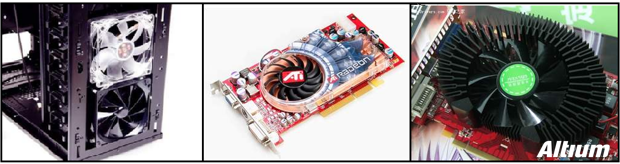
1Using Thicker Copper for High Current
Resistance in copper traces and vias can lead to significant power loss and heat generation in PCB-based devices, especially when they carry large currents. Electrical connections with a larger cross-sectional area have lower resistance, which reduces the amount of heat loss. Most PCBs use a copper thickness equivalent to about 1 ounce per square foot. When it is inconvenient to use fans or heat sinks, increasing the copper thickness can be a solution. A high-current PCB should use at least double the amount of copper. Circuits with operating currents exceeding 10 amps should have copper thicknesses of up to 3 or 4 ounces per square foot. The copper thickness of PCB boards is measured in oz, where 1 oz means the weight of copper foil averaged over an area of 1 square foot is 28.35g. Conversion method: The weight of the copper foil divided by the density of copper and the surface area gives the thickness of the copper foil. 1 square foot = 929.0304 square centimeters, copper density = 8.9kg/dm^3 Let Copper thickness be X, solving the equation: X*929.0304 square centimeters*8.9 grams/cubic centimeter = 1oz = 28.35 grams X=0.0034287 centimeters = 34.287um Therefore, 1oz = 34.287um. The thickness of 1OZ copper foil is about 35um or 1.35mil. 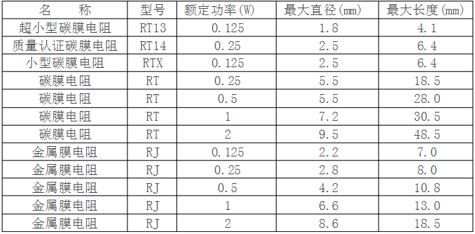 The above figure shows the current capacity versus trace width curve for a 1oz copper thickness PCB. For reference.Using a larger amount of copper will require increasing the width of traces on the PCB. To avoid occupying too large a space area, traces can also be embedded deeper within the circuit board. For example, by placing copper bars. This also helps dissipate heat into the circuit board itself and any nearby heat dissipation holes. Of course, this may require using thicker circuit boards, which is suitable for high-current devices.
2Using Heat Sinks and Thermal Pads
Air around heat-generating components cannot effectively dissipate heat without flow. Using heat sinks can transfer heat away from critical electronic components on the circuit board. Thermal vias are good heat conduction components between the top and bottom layers of the circuit board. Heat can be transferred to thermal vias through simple conduction, and then the thermal vias can dissipate heat away from critical electronic components. Thermal pads are generally a metal plate installed on the bottom layer of the circuit board. After thermal vias transfer heat away from the hottest spots of the circuit board, they must go to other locations to further dissipate heat from the hottest spots of the circuit board. Generally, thermal vias transfer heat to thermal pads for large-area heat dissipation. The following image shows an infrared image of a PCB operating under high current: 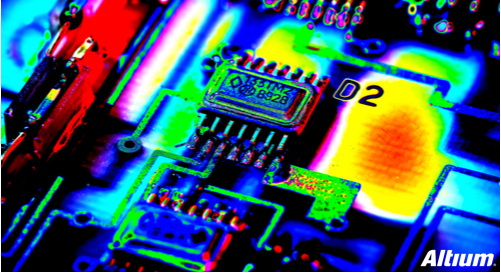
3Layout of High-Power Components
High-current electronic components like microcontrollers generate a lot of heat. It is a good idea to install these components near the center of the circuit board. If components are installed near the edges of the circuit board, the heat they generate will accumulate, and local temperatures can become very high. However, if components are installed in the middle of the circuit board, heat will dissipate throughout the entire circuit board, reducing the temperature of the PCB. Multiple high-power components should be dispersed across the entire circuit board rather than concentrated in one location. If the size of the components allows, different components can even be separated onto different PCBs. When laying out components, careful consideration is required, as it relates to the functionality of the entire circuit board, heat dissipation, and mechanical matching, as well as the potential impact on your manufacturing budget. 
4Using Thicker Boards
When components operate at extreme temperatures, the lifespan of their electrical connections, components, and the circuit board itself will be shortened accordingly. The computer hardware industry has reduced the risk of this issue with cooling fans. However, when fans are not effective, most heat directly enters the circuit board and surrounding components. If the circuit board is thin at this time, everything will heat up to very high temperatures.Thicker circuit boards will require more heat energy when the overall temperature rises. Thus, thicker circuit boards help keep the temperature at the top of the circuit board lower. If the circuit board is directly mounted to the housing, it can conduct heat to the outside of the device. However, this solution may increase production costs, so it is necessary to weigh this appropriately when applying it. Below, we show some different board thicknesses used in some of our previous hardware. 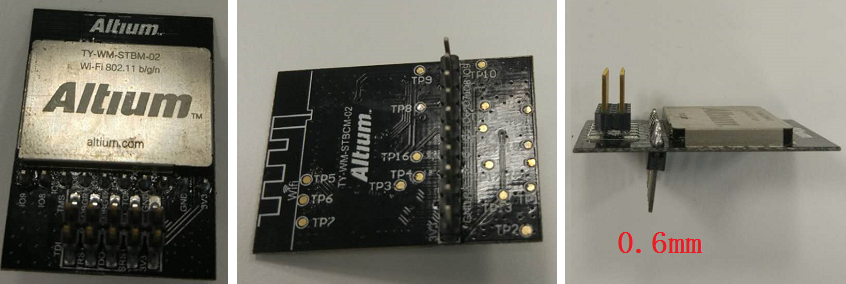 The above image shows a WiFi module used in an IoT project with a board thickness of 0.6mm.
 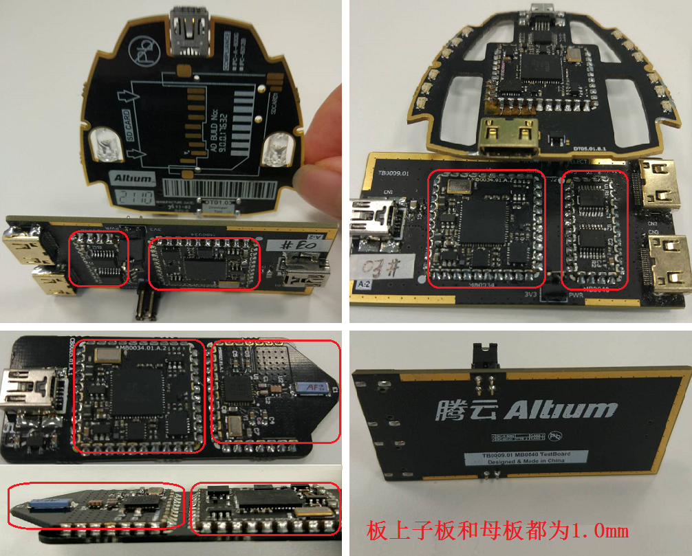 The above image shows a JTAG-USB adapter for FPGA hardware development, as well as other signal conversion modules, which are not high-current, high-heat circuits. The board thickness is 1.0mm. The sub-board on the board serves as a small module for similar components, with half holes, edge gold-plated, and the entire board is soldered to the motherboard. Both the sub-board and motherboard are 1.0mm thick.
 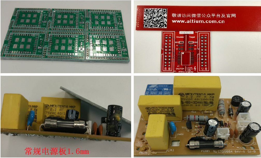 The above image shows a conventional power board with a thickness of 1.6mm. This 1.6mm is the default thickness of most board manufacturers, and unless specified otherwise, it is assumed to be this thickness. Moreover, the processing cost for 1.6mm is the critical point. There are no additional costs for special thicknesses below 1.6mm.
 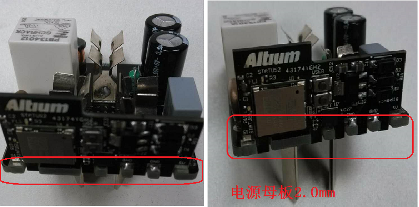 The above image shows a power socket with a WiFi module that can be remotely controlled. The motherboard power board has a thickness of 2.0mm. The 2.0mm is a thick board manufacturing process. This thickness is designed considering the situation of high heat generation due to large currents in small spaces.The best heat dissipation strategy to adopt depends on many factors. Not all design or form factors can accommodate all of the above strategies. For example, thermal pads are not suitable for double-sided printed circuit boards. If there are many components on the circuit board, some components will inevitably need to be placed near the edges of the circuit board. Copyright statement: This article is copyrighted by the original author and does not represent the views of the association. The articles promoted by the “Jiangxi Province Electronic Circuit Industry Association” are for sharing purposes only and do not represent the stance of this account. If there are copyright issues, please contact us for deletion.