With the continuous development of electronic science and technology, PCB technology has also undergone tremendous changes, and manufacturing processes need to progress as well. At the same time, the requirements for PCB circuit board processes in various industries have gradually increased. For example, circuit boards in mobile phones and computers use both gold and copper, making it easier to distinguish the quality of circuit boards.
Today, we will explore the surface processes of PCB boards and compare the advantages and disadvantages of different PCB surface treatment processes and their applicable scenarios.

From a purely external perspective, the outer layer of the circuit board mainly comes in three colors: gold, silver, and light red. Classified by price: gold is the most expensive, silver is the second most expensive, and light red is the cheapest. From the color, it is actually easy to judge whether the hardware manufacturer is cutting corners. However, the internal lines of the circuit board are primarily pure copper, which is a bare copper board.
1. Bare Copper Board
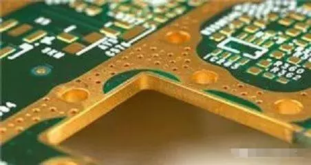
The advantages and disadvantages are obvious:
Advantages: low cost, smooth surface, good solderability (if not oxidized).
Disadvantages: easily affected by acid and humidity, cannot be stored for long, needs to be used within 2 hours after unsealing, as copper exposed to air is prone to oxidation; cannot be used for double-sided boards because the second side will already be oxidized after the first reflow soldering. If there are test points, solder paste must be printed to prevent oxidation; otherwise, it will not be able to make good contact with the probe later.
Pure copper is easily oxidized when exposed to air, so the outer layer must have the protective layer mentioned above. Moreover, some people mistakenly believe that the golden color is copper, which is incorrect, as that is the protective layer on top of the copper. Therefore, it is necessary to plate gold extensively on the circuit board, which is the immersion gold process I previously discussed.
2. Gold-Plated Board
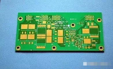
The gold color is real gold. Even if it is only a very thin layer, it accounts for nearly 10% of the circuit board’s cost. In Shenzhen, there are many merchants who specialize in purchasing waste circuit boards and extract gold through certain means, which is a nice income.
The use of gold as a plating layer is primarily for ease of soldering and to prevent corrosion. Even after years of use, the gold fingers of memory sticks still shine as before. If copper, aluminum, or iron had been used, they would have rusted into a pile of scrap.
The gold plating layer is widely used in the pads of circuit board components, gold fingers, and connector springs. If you find that the circuit board is actually silver, there is no need to say more; just call the consumer rights hotline, as the manufacturer has definitely cut corners and failed to use proper materials, using other metals to deceive customers. The mainboards of mobile phone circuit boards we use most widely are mostly gold-plated boards, while computer motherboards, speakers, and small digital circuit boards are generally not gold-plated.
The advantages and disadvantages of the immersion gold process are not difficult to deduce:
Advantages: not easily oxidized, can be stored for a long time, smooth surface, suitable for soldering fine pitch pins and small components. It is the first choice for key PCB boards (such as mobile phone boards). It can be repeatedly passed through reflow soldering without significantly reducing its solderability. It can be used as a substrate for COB (Chip On Board) wire bonding.
Disadvantages: higher cost, weaker solder joint strength, as it uses a non-electrolytic nickel process, which can easily lead to black pad issues. The nickel layer will oxidize over time, raising long-term reliability concerns.
Now we know that the golden color is gold, and the silver color is not silver, but tin.
3. Tin-Sprayed Circuit Board
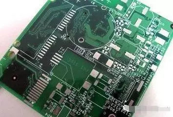
The silver board is called a tin-sprayed board. A layer of tin is sprayed on the outer layer of the copper lines, which can help with soldering. However, it cannot provide long-term contact reliability like gold. It has no impact on already soldered components, but for pads exposed to air for a long time, the reliability is insufficient, such as grounding pads and spring sockets. Long-term use is prone to oxidation and rust, leading to poor contact. Basically, all circuit boards used for small digital products are tin-sprayed boards, as they are cheap.
Its advantages and disadvantages can be summarized as:
Advantages: lower price, good soldering performance.
Disadvantages: not suitable for soldering fine pitch pins and very small components, as the surface flatness of the tin-sprayed board is relatively poor. In PCB processing, solder beads can easily form, which can cause short circuits for fine pitch components. When used in double-sided SMT processes, since the second side has already undergone high-temperature reflow soldering, it is very easy for the tin spray to remelt, causing solder beads or similar droplet-like solder points to form under the influence of gravity, resulting in a more uneven surface and thus affecting the soldering quality.
I previously mentioned the cheapest light red circuit board, which is a thermoelectric separation copper substrate for miner’s lamps.
4. OSP Process Board
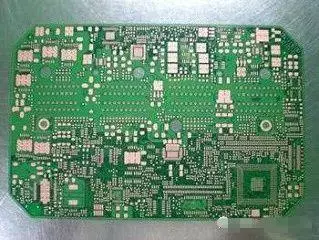
Organic Solder Mask. Since it is organic and not metal, it is even cheaper than the tin-spray process.
Its advantages and disadvantages are:
Advantages: possesses all the advantages of bare copper board soldering, and expired boards can be reprocessed.
Disadvantages: easily affected by acid and humidity. When used in secondary reflow soldering, it needs to be completed within a certain time, and typically the effect of the second reflow soldering will be poorer. If stored for more than three months, it must be reprocessed. After unsealing, it must be used within 24 hours. OSP serves as an insulating layer, so solder paste must be printed on the test points to remove the original OSP layer to allow contact with the probe for electrical testing.
The only function of this organic film layer is to ensure that the inner copper foil does not oxidize before soldering. When heated during soldering, this layer evaporates, allowing solder to bond the copper lines and components together.
However, it is not very corrosion-resistant; an OSP circuit board exposed to air for about ten days can no longer have components soldered onto it.
Many computer motherboards use OSP processes because the area of the circuit board is too large to afford gold plating.
Disclaimer:All rights to this article are owned by the original author and do not represent the views of the association.The articles promoted by the “Jiangxi Province Electronic Circuit Industry Association” are for sharing purposes only and do not represent the position of this account. If there are copyright issues, please contact us for deletion.