Continuing from the previous article on MOSFETs, this one will still take the enhanced NMOS as an example.
We know that NMOS operates in several regions: cutoff region, linear region, saturation region, and breakdown region. The operating current of the MOSFET is related to the threshold voltage Vth. So, what parameters are related to the threshold voltage Vth? Refer to the following formula.
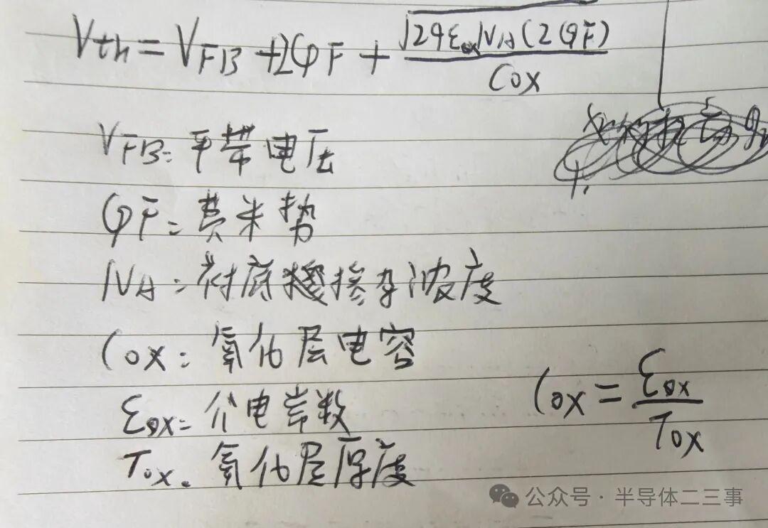
Flat Band Voltage Vfb: The gate voltage required to offset the work function difference between the metal (or polysilicon) gate and the semiconductor substrate, as well as the influence of fixed charges in the oxide layer, is the “baseline” for Vth. Formula: VFB = Φms – (Qox / Cox). This includes two parts: the first part is the metal-semiconductor work function difference Qms, which is determined by the inherent properties of the gate material (such as N+ polysilicon, P+ polysilicon, or metal) and the substrate material (P-type or N-type silicon). This is one of the main determinants of Vth. The second part is the influence of fixed charges in the oxide layer (Qox), which are positive charges generated during the manufacturing process of the SiO2 oxide layer. These positive charges help attract electrons, thus reducing the Vth of the NMOS (making it easier to turn on).
Fermi Potential: The surface potential energy required to achieve strong inversion at the surface. Here, φF is the Fermi potential of the substrate, which is related to the substrate doping concentration (Na).
Substrate Doping Concentration Na: For NMOS, this refers to the doping concentration of the P substrate.
Unit Area Oxide Capacitance Cox: This is proportional to the dielectric constant of the oxide layer and inversely proportional to the thickness of the oxide layer.
Oxide Layer Dielectric Constant εox: To increase Cox, high-k dielectrics can be used, such as hafnium oxide HfO2, which has a k value about 6 times that of SiO2.
Oxide Layer Thickness Tox: As the size of the MOSFET shrinks, Tox also needs to shrink proportionally to maintain the gate’s control over the channel. However, if the oxide layer Tox is too thin, quantum tunneling effects can easily occur, leading to significant gate leakage current and a sharp increase in power consumption. According to the formula Cox = εox / Tox, to achieve the same unit area capacitance, for high-k dielectrics, a thicker physical layer can be used (Tox can be larger), and a thicker physical layer can effectively suppress quantum tunneling, significantly reducing gate leakage current while maintaining the device’s drive capability.