In yesterday’s tweet, we discussed the impact of the bit depth of microcontroller ADCs on measurement errors. It should be noted that the experiments mentioned in the tweet were merely for theoretical validation. As suggested by a netizen later: the performance of microcontroller ADCs (ENOB and non-linearity) can only be verified through experimental data when the power supply and decoupling are correctly ensured.
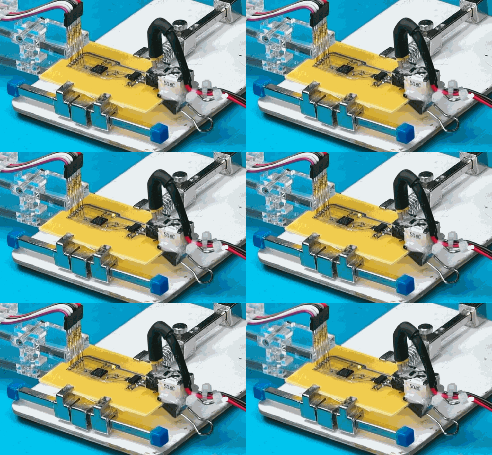 Especially, in terms of circuit board manufacturing and layout, careful consideration is required. In this regard, invited by Jialichuang, I will introduce the basic knowledge of the process flow for high multi-layer PCB manufacturing. At the end of the article, you can find information about Jialichuang’s exclusive coupon for PCB 6-32 layer circuit boards (for first-time users).
01.
High Multi-Layer PCB Materials
1. High Multi-Layer PCB Materials account for 60% of PCB costs, making the choice of good materials crucial for PCB production. A good material primarily exhibits extraordinary performance in the following three aspects.(1) The conductivity of the copper foil and the dielectric performance of the insulating material are key to improving signal transmission speed, reducing signal attenuation, and minimizing circuit crosstalk noise.(2) The PCB materials need to have better thermal conductivity and a low thermal expansion coefficient, which can optimize the thermal conduction distribution of the circuit and avoid the generation of hotspots and the accumulation of thermal stress.(3) As the number of layers and the size of the circuit board increase, the circuit board needs to have better mechanical strength and stability, which enhances the rigidity and durability of the material, ensuring circuit stability in environments subject to vibration, impact, and bending.
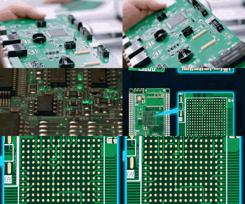
2. Types of High Multi-Layer PCBs
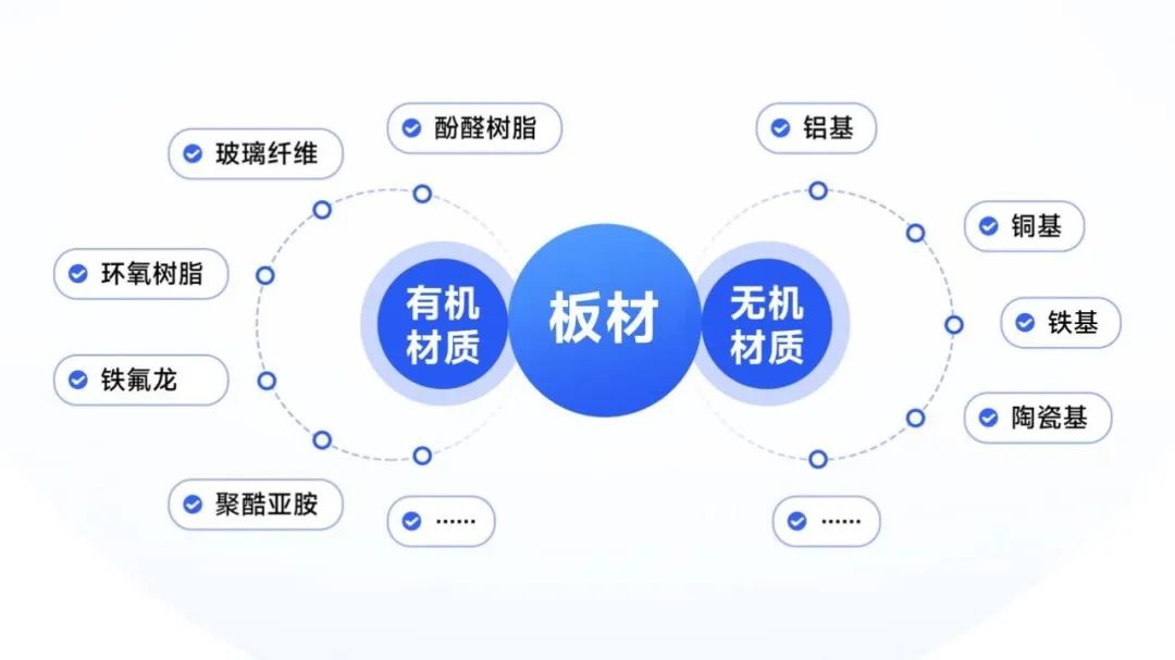
The basic material for PCB production is Copper Clad Laminate (CCL), which is a key raw material for high multi-layer PCBs. It is composed of copper foil, resin, fiberglass cloth, and other functional additives. By immersing the reinforcing materials in resin and applying copper foil on one or both sides, it is formed into sheet materials through hot pressing. In classification, materials can be distinguished based on dimensions such as material type, finished hardness, structure, and grade.Specifically, materials can be divided into two main categories: organic and inorganic materials.
Structurally, materials can be classified into single-sided, double-sided, multi-layered, and HDI (High-Density Interconnect boards, characterized by blind and buried via technology).3. Key Points in Choosing PCBsThe selection of PCB materials is often easiest from an appearance perspective, avoiding defects such as dents, wrinkles, scratches, and bubbles on the metal foil surface. Additionally, dimensions such as length, width, diagonal deviation, and warpage must ensure the assembly precision and performance of the PCB.
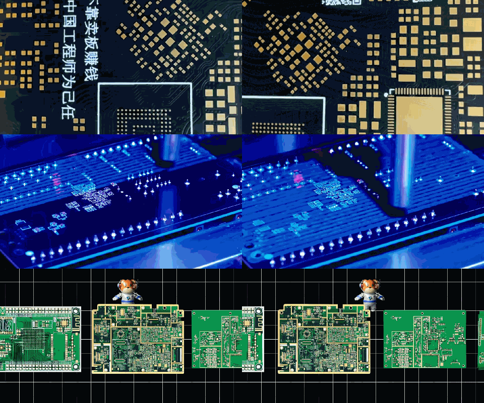
Besides visible appearance, electrical performance, thermal performance, and mechanical performance are also important.(1) Electrical performance.Electrical performance includes dielectric constant (Dk), dissipation factor (DF), volume resistivity, surface resistivity, insulation resistance, arc resistance, breakdown voltage, electrical strength, and comparative tracking index (CTI).(2) Thermal performance.Thermal performance mainly involves Tg value, Td value, CTE, thermal stress, combustibility, etc.(3) Physical (mechanical) performance.In terms of physical mechanical performance, the quality and applicability of PCB materials are influenced by various factors, including copper foil peel strength, flexural strength, water absorption, combustibility, etc.
02.
High Multi-Layer PCB Manufacturing Process
The process of making multi-layer PCBs can refer to the diagram below. Compared to single and double-sided PCBs, high multi-layer PCBs have an additional inner layer process.
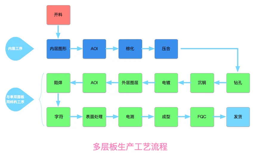
Although the multi-layer process is relatively complex, it is all handled by Jialichuang. From the user’s perspective, all that is needed is to submit the production information files, including Gerber files, drilling files, netlist data, etc. After the PCB manufacturing company reviews and confirms the production information, the PCB factory will adjust the PCB design routing information based on its manufacturing processes, such as via drill diameter compensation or trace etching compensation, to enhance the manufacturability of the PCB. Some critical modifications may also require communication with the PCB layout team for confirmation.
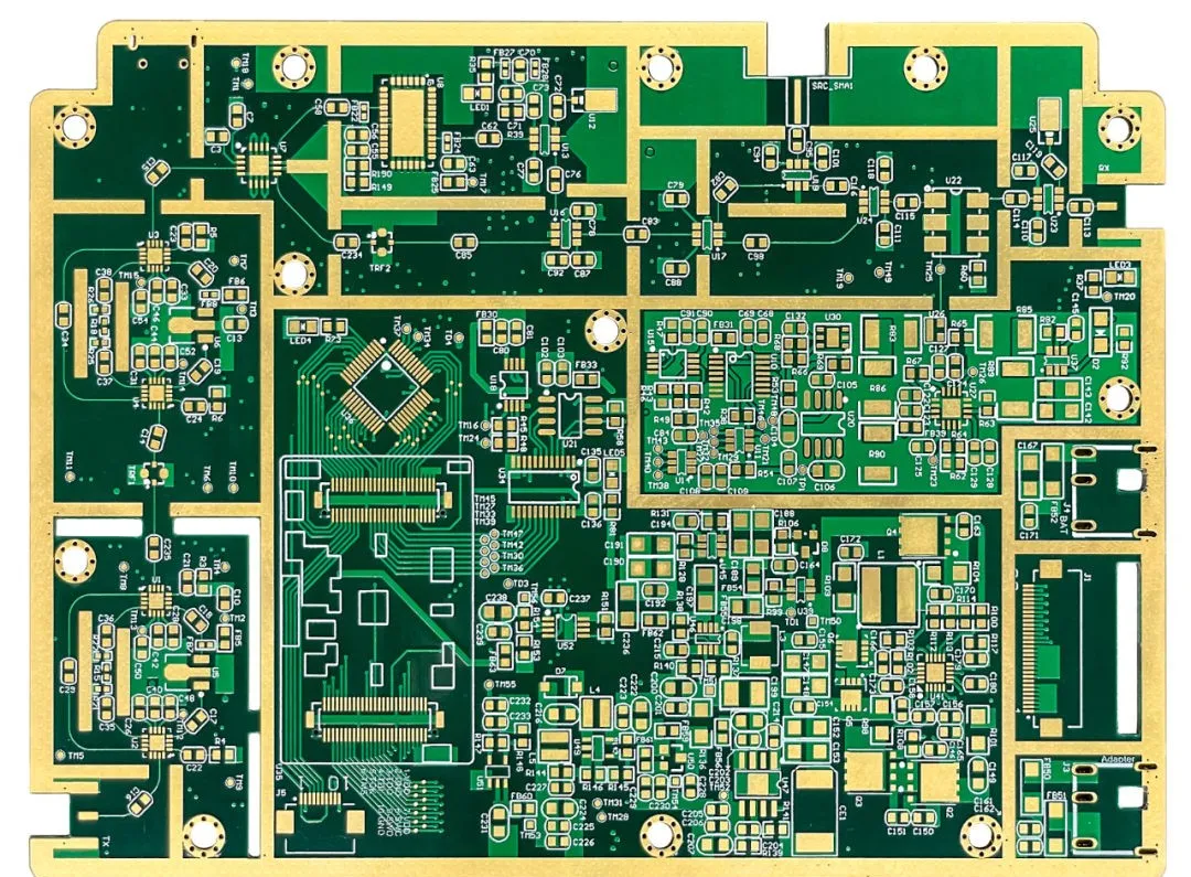
If you are using Jialichuang for PCB production, they also offer a personalized service called “Confirm Production Draft,” which allows us to carefully check and identify any issues in our design, and of course, to spot any errors made by Jialichuang’s engineers during the process. If it is Jialichuang’s fault, don’t forget to ask the engineers to refund the confirmation fee for the production draft. Next, we begin selecting materials and the multi-layer board production process.
Incredibly, the production of multi-layer boards typically requires about 200 different processing steps. Therefore, it is very important for PCB designers to be familiar with the various types and properties of substrates, the manufacturing process of multi-layer boards, and the soldering process.One of the significant factors affecting the quality of the multi-layer board structure is the precise alignment between the different layers. These layers must be accurately overlapped; otherwise, circuit short-circuiting or opening problems may arise after drilling connections. Precise alignment is achieved through mechanical alignment holes, and positioning pins are used during lamination to adjust the layers.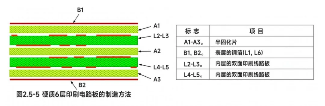 The image above is a schematic of the manufacturing of a 6-layer rigid multi-layer board. A1, A2, A3 are prepregs, L2-L3, L4-L5 are double-sided copper-clad laminates that complete the inner layer patterns, and B1, B2 are copper foils used for the outer layer circuits.
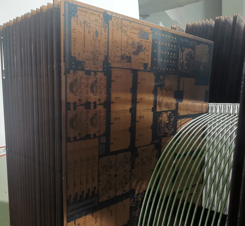
As shown in the image above, the PCB design draft is ultimately assembled onto a large working panel for production. For characteristic impedance control, the uniformity of resin flow during lamination of the entire large panel also significantly impacts impedance variation, making the performance of the lamination equipment crucial.
03.
Gold Plating and Via-in-Pad
The need for multi-layer boards essentially arises from issues caused by circuit density. To this end, Jialichuang employs gold plating, via-in-pad technology, and positive photoresist process, providing comprehensive assurance for circuit layout and production.
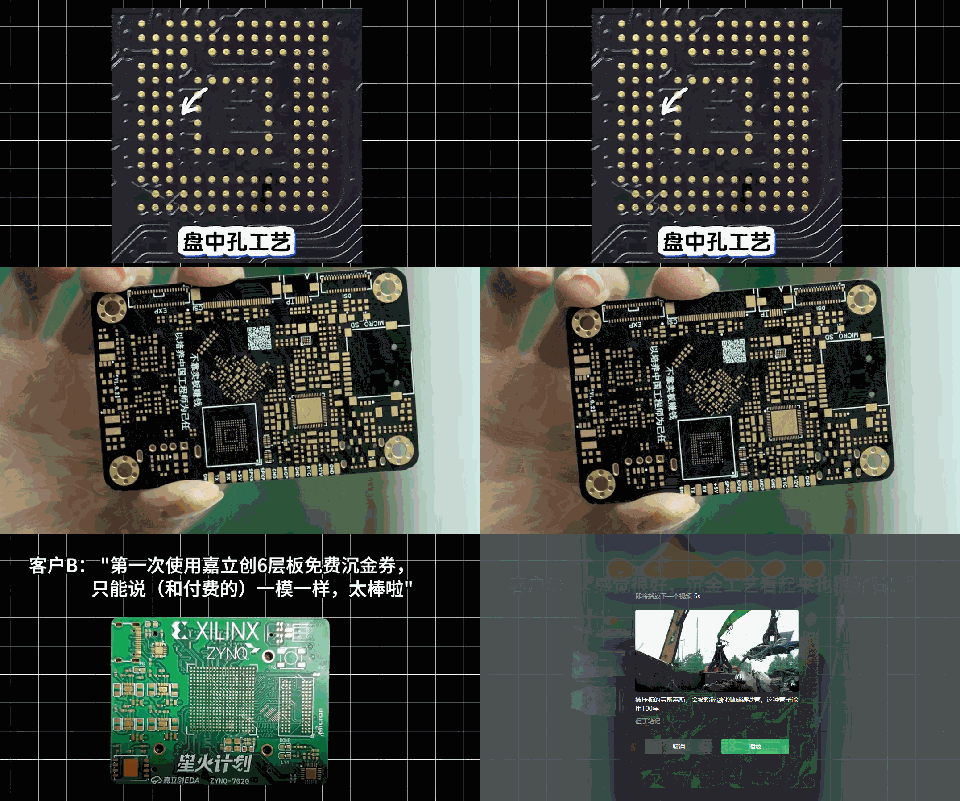
Gold is so expensive, but Jialichuang is willing to invest in gold plating on circuit boards. The 2U” gold plating not only enhances the electrical conductivity of the circuit board but also establishes a flat base on the surface of all pads, improving the soldering quality of surface-mounted devices and extending the lifespan of the PCB.
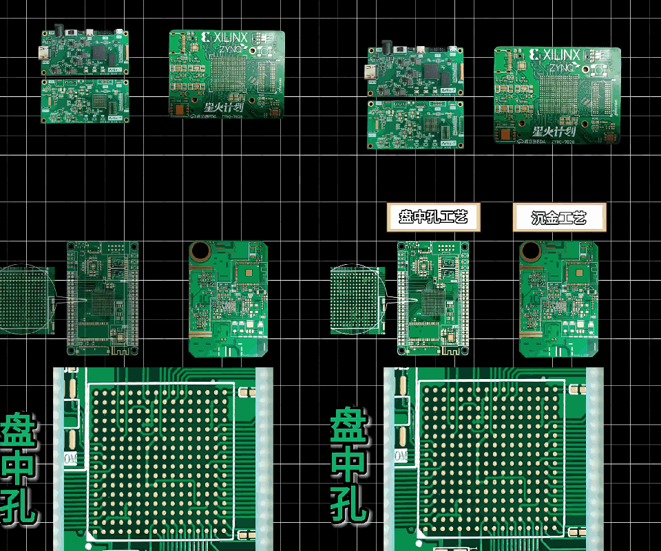
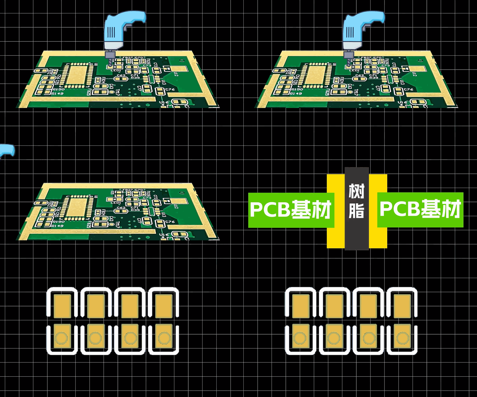
Jialichuang’s via-in-pad technology is also remarkable, effectively solving the wiring issues of high-density BGA components, while simultaneously ensuring smoother signal transmission and faster heat dissipation. It addresses signal attenuation and leakage, enhancing circuit reliability.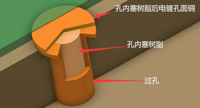
3D diagram of via-in-pad technology
Historically, via-in-pad technology has mainly been applied to high-end products and has been quite expensive. Now, Jialichuang offers it for free, allowing via-in-pad technology to become accessible to the general public, enabling more customers to enjoy higher quality craftsmanship and obtain more reliable products.
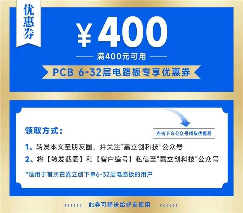
Now it’s time to distribute benefits; below is the exclusive coupon for high multi-layer PCBs provided by Jialichuang. You can follow the “Redemption Method” in the image to obtain the PCB discount coupon.
 Indeed, Jialichuang’s high multi-layer PCBs are excellent, and the discounts and free offerings are appealing, but they cannot solve all problems encountered in electronic experiments. One of the issues is time; for simple circuit experiments, one-minute PCB production allows us to get what we want immediately, while the formal production process takes several days. Below is a netizen’s candid remark about one-minute PCB production: Although the microcontroller I purchased has arrived, the PCB is still on its way via express delivery. Fortunately, I don’t have a laser printer; otherwise, I would definitely be tempted to buy hydrogen peroxide by now.
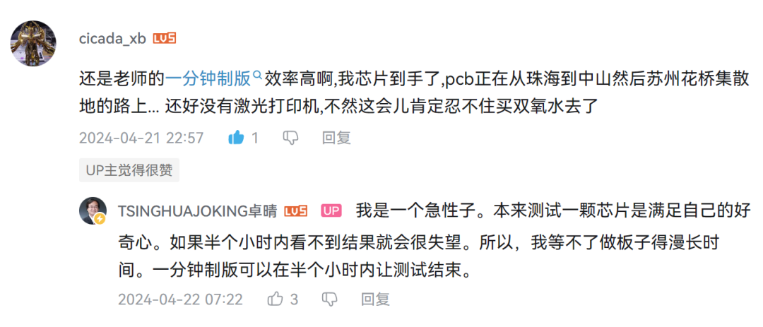
It seems that there are many people in this world, just like me, impatient and eager to have hot tofu.