The CDC (Cross-Clock Domain) issue is a core topic in FPGA/Digital IC interviews. Since most students’ FPGA/Digital IC projects primarily involve synchronous clock processing, many people still have a theoretical understanding of CDC issues, and they struggle to respond when the question type changes.This series of articles will delve into CDC issues, introducing CDC handling, CTS, and CDC timing constraints. Interested readers are encouraged to follow along.1. Synchronous Clock or Asynchronous Clock?In digital systems, the attributes of a clock include: frequency, phase, and clock source. Therefore, the key point in distinguishing between synchronous and asynchronous clocks is whether the frequency and phase relationship of each clock is fixed and whether the clocks are from the same source (having predictability).1.1 What is a Synchronous Clock?A synchronous circuit is one where the entire design uses the same clock source, and the frequency and phase relationships between the clocks are known in advance, as shown in the following clocks:
- Same frequency and same phase
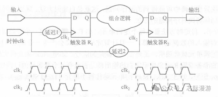
- Same frequency but different phase (fixed phase difference): usually caused by clock path delay leading to Clock Skew
- Same source but different frequency (integer multiple frequency ratio): divided clocks or integer multiple clocks output from the same PLL
It is important to note that in certain situations (which will be explained in detail later), even if the source and destination belong to synchronous clocks, cross-clock domain processing is still required to ensure that data is transmitted correctly.The advantage of synchronous design is that EDA tools can easily perform timing checks on fully synchronous designs; on the other hand, synchronous designs have the characteristic of clock edge sampling, which can prevent glitches from propagating throughout the circuit.1.2 What is an Asynchronous Clock?An asynchronous clock is one where the clocks are from different sources (outputs from two PLLs or outputs from different oscillators), or the clocks are from the same source but have a non-integer multiple frequency ratio (which causes the phase relationship between the two clocks to be unpredictable), as shown in the following clocks:
- Different sources: Clocks from different oscillators or PLL outputs, with an unclear phase relationship
- Same source but different frequency (non-integer multiple frequency ratio): divided clocks or integer multiple clocks output from the same PLL
2. Why Do Asynchronous Designs Occur? When is Cross-Domain Processing Required?In summary: It is done out of necessity. The disadvantages of fully synchronous designs mainly manifest in these two aspects:1. In complex digital designs (such as SoC systems), various low-speed modules (like UART) and high-speed modules (like CPU, GPU) are often integrated, making it nearly impossible to use the same clock, leading to the adoption of GALS (Globally Asynchronous/Locally Synchronous) designs;
For example, a CPU core with a core frequency of 1GHz typically has a JTAG interface for debugging that does not exceed 20MHz, so asynchronous processing circuits must be designed between the CPU and JTAG (to allow safe interaction of debug information between the 1GHz and 20MHz clock domains).
2. The Clock Skew issue, where the clock edges arrive at each Flip-Flop at different times (as shown in the diagram below with clk1 and clk2; CTS (Clock Tree Synthesis) can solve this problem, but it requires inserting delay elements into low-latency clock paths, which inevitably increases area and power consumption);
 3. The same source but different frequency (integer multiple frequency ratio) situation may not appear to cross the clock domain. However, when the slow clock samples the fast clock, the fast clock’s rapid transitions can lead to the slow clock failing to correctly sample the fast clock’s data. In this case, processing is also required to widen the fast clock signal so that the slow clock domain can correctly sample.
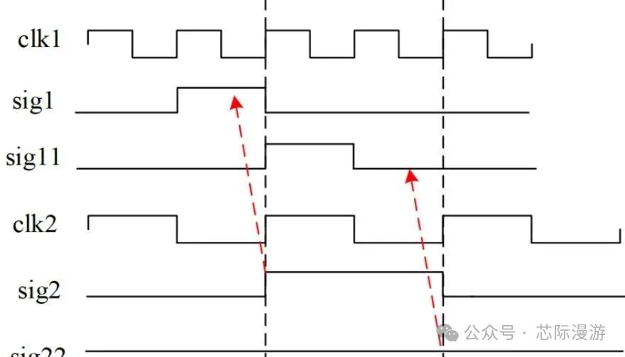 It is essential to clarify that the core goal of cross-clock domain processing is to ensure that data can be correctly transmitted from the source to the destination. In the next article, we will discuss the metastability issue.Follow Chip Journey on WeChat for more digital IC/FPGA learning materials and autumn recruitment information.
Autumn Recruitment Real Questions:
1. When transferring data from a high-frequency clock domain (which changes every clock cycle) to a low-frequency clock domain, which synchronization method is correct? ( ).
A. Use handshake signals for synchronizationB. Use asynchronous FIFOC. Use synchronous FIFOD. Use two-pulse synchronization
Answer: B. Fast clock data changes every cycle, so it cannot be captured by the slow clock through pulse widening, hence using asynchronous FIFO to buffer the data.
2. When signals cross clock domains, metastability occurs. What factors are related to its failure? ( ).
A. The flip-flop output signal flip rate at the signal transmitterB. The clock frequency of the signal transmitter’s registerC. The clock frequency of the signal receiver’s registerD. The number of synchronous registersAnswer: A, B, C, D.Previous Highlights:【Autumn Recruitment】Huawei Logic Special Session, Logic/Digital IC/FPGA – Interview Point Analysis (3) STA Static Timing Analysis【Autumn Recruitment】Huawei Logic Special Session, Logic/Digital IC/FPGA – Interview Point Analysis (1) HDL Basics and Timing Constraints【Autumn Recruitment】Huawei Logic Special Session, Logic/Digital IC/FPGA – Interview Point Analysis (2) SV Basics