Welcome FPGA engineers to join the official WeChat technology group.
Clickthe blue wordsto follow us at FPGA Home – the largest and best pure FPGA engineer community in China.
The interface between Field Programmable Gate Arrays (FPGA) and Analog-to-Digital Converters (ADC) digital data output is a common engineering design challenge. This article briefly introduces various interface protocols and standards, and provides tips and tricks for using LVDS in high-speed data converter implementations.
Interface Methods and Standards The interface between Field Programmable Gate Arrays (FPGA) and Analog-to-Digital Converters (ADC) digital data output is a common engineering design challenge. Moreover, ADCs use a variety of digital data styles and standards, making this challenge even more complex. For low-speed data interfaces typically below 200 MHz, Single Data Rate (SDR) CMOS is very common: the transmitter sends data on one clock edge, while the receiver receives data on another clock edge. This method ensures that there is sufficient time for the data to settle before being sampled by the receiver. In Double Data Rate (DDR) CMOS, the transmitter sends data on every clock edge. Therefore, it transmits twice the amount of data in the same time as SDR. However, the timing for the receiver to sample correctly is more complex.
Parallel Low Voltage Differential Signaling (LVDS) is a common standard for high-speed data converters. It uses differential signals, with each bit having a P line and an N line; in the latest FPGAs, speeds can reach DDR 1.6 Gbps or 800 MHz. Parallel LVDS consumes less power than CMOS, but requires twice as many lines as CMOS, making routing more challenging.
LVDS is often used in data converters with a “source-synchronous” clock system, although this is not part of the LVDS standard. In this setup, the clock is in phase with the data and is sent along with the data. This allows the receiver to capture data more easily using the clock, as it now knows when the data transfer occurs.
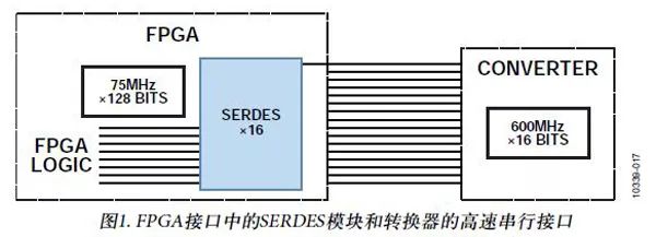
The speed of FPGA logic generally does not keep up with the bus speed of high-speed converters, so most FPGAs have Serializer/Deserializer (SERDES) modules to convert the fast, narrow-band serial interface at the converter end to a slower, wide-band parallel interface at the FPGA end. For each data bit in the bus, this module outputs 2, 4, or 8 bits, but at ½, ¼, or 1/8 the clock rate, effectively deserializing the data. The data is processed internally by the FPGA’s wide bus, which operates at a speed much lower than the narrow bus connected to the converter.
The LVDS signal standard is also used for serial links, mostly in high-speed ADCs. When the number of pins is more important than the interface speed, serial LVDS is typically used. Two clocks are often used: the data rate clock and the frame clock. All considerations mentioned for parallel LVDS also apply to serial LVDS. Parallel LVDS is simply composed of multiple serial LVDS lines.
I2C uses two lines: clock and data. It supports a large number of devices on the bus without additional pins. I2C is relatively slow, with speeds ranging from 400 kHz to 1 MHz, considering protocol overhead. It is typically used for slow, small devices. I2C is also often used as a control interface or data interface.
SPI uses 3 to 4 lines:
-
Clock
-
Data input and data output (4 lines), or bidirectional data input/output (3 lines)
-
Chip select (one line for each non-master device)
The number of available chip select lines determines how many devices SPI can support. Its speed can reach about 100 MHz, and it is typically used as a control interface and data interface.
Serial PORT (SPORT) is a bidirectional interface based on CMOS, using one or two data pins for each direction. Its adjustable word length can improve efficiency for non-8-bit resolutions. SPORT supports Time Domain Multiplexing (TDM) and is typically used in audio/media converters and high-channel count converters. It provides performance of about 100 MHz per pin.
Blackn processors support SPORT, and SPORT can be implemented directly on FPGA. SPORT is generally used only for data transmission, but control characters can also be inserted.
JESD204 is a JEDEC standard for high-speed serial links between a single host (such as FPGA or ASIC) and one or more data converters. The latest specifications provide speeds of up to 3.125 Gbps per channel or per differential pair. Future versions may provide speeds of 6.25 Gbps and higher. Channels use 8B/10B encoding, so the effective bandwidth of the channel is reduced to 80% of the theoretical value. The clock is embedded in the data stream, so no additional clock signal is needed. Multiple channels can be combined to increase throughput, and the data link layer protocol ensures data integrity. In FPGA/ASIC, the resources required for JESD204 to achieve data frame transmission far exceed those for simple LVDS or CMOS. It significantly reduces wiring requirements but requires more expensive FPGAs and more complex PCB routing.
General Recommendations When designing the interface between ADC and FPGA, the following general recommendations may be helpful.
-
Use external resistor termination for the receiver, FPGA, or ASIC, rather than using the internal termination of the FPGA, to avoid reflections caused by mismatches that exceed timing budgets.
-
If the system uses multiple ADCs, do not use a specific DCO from one ADC.
-
When laying out digital traces connected to the receiver, avoid excessive “tromboning” to keep all traces
equal length.
-
Use series termination at the CMOS output to reduce edge rates and limit switching noise. Confirm that the data format used (two’s complement or offset binary) is correct.
When using single-ended CMOS digital signals, logic levels move at a speed of about 1 V/nS, with a typical output load of 10 pF (maximum), and a typical charging current of 10 mA/bit. The capacitive load should be as small as possible to minimize the charging current. This can be achieved by driving a gate with the shortest trace possible, preferably without any vias. Damping resistors can also be used at the digital output and input to minimize charging current.
The time constant of the damping resistor and capacitive load should be about 10% of the sampling rate period. If the clock rate is 100 MHz and the load is 10 pF, then the time constant should be 10 nS’s 10%, which is 1 nS. In this case, R should be 100 Ω. For optimal signal-to-noise ratio (SNR) performance, 1.8 V DRVDD is better than 3.3 V DRVDD. However, when driving large capacitive loads, SNR performance may degrade. CMOS output supports sampling clock rates of up to about 200 MHz. If driving two output loads or if the trace length exceeds 1 or 2 inches, a buffer is recommended.

ADC digital outputs should be handled with care, as transient currents can couple back to the analog input, increasing noise and distortion in the ADC.
A typical CMOS driver, as shown in Figure 2, can generate large transient currents, especially when driving capacitive loads. Special measures must be taken for CMOS data output ADCs to minimize these currents to avoid introducing extra noise and distortion in the ADC.
Typical Examples
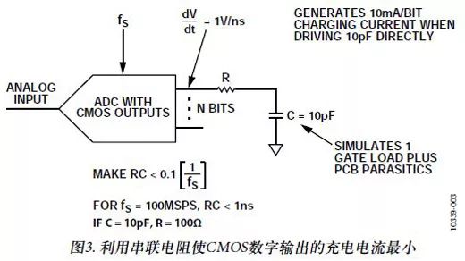
Figure 3 shows the case of a 16-bit parallel CMOS output ADC. Each output has a 10pF load to simulate a gate load plus PCB parasitic capacitance; when driving a 10 pF load, each driver generates a charging current of 10 mA. Thus, the total transient current of this 16-bit ADC can be as high as 16 × 10 mA = 160 mA. Adding a small series resistor R at each data output can suppress these transient currents. The value of this resistor should be chosen appropriately to ensure that the RC time constant is less than 10% of the total sampling period. If fs = 100 MSPS, then RC should be less than 1 ns. C = 10 pF, so the optimal R value is about 100 Ω. Choosing a larger R value may degrade output data setup time performance and interfere with normal data capture. The capacitive load at the CMOS ADC output should be limited to a single gate load, typically an external data capture register. In any case, the data output should not be directly connected to a high-noise data bus; an intermediate buffer register must be used to minimize the direct load on the ADC output.
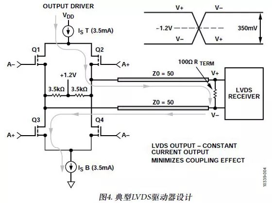
Figure 4 shows a standard LVDS driver in CMOS. The nominal current is 3.5 mA, with a common mode voltage of 1.2 V. Thus, when driving a 100 Ω differential termination resistor, the swing at each input of the receiver is 350 mV p-p, which corresponds to a differential swing of 700 mV p-p. These values come from the LVDS specification.
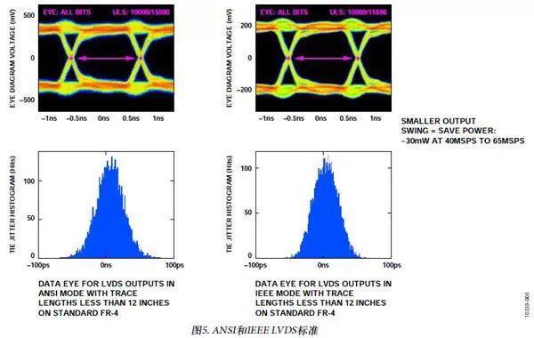
There are two LVDS standards: one established by ANSI and the other by IEEE. Although these two standards are similar and generally compatible, they are not identical. Figure 5 compares the eye diagrams and jitter histograms of these two standards. The swing of IEEE standard LVDS is 200 mV p-p, lower than the 320 mV p-p of the ANSI standard, which helps to save power in digital outputs. Therefore, if the IEEE standard supports the target application and connection with the receiver, it is recommended to use the IEEE standard.
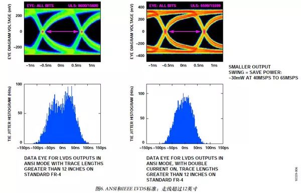
Figure 6 compares the ANSI and IEEE LVDS standards in cases where the trace length exceeds 12 inches or 30 cm. In both figures, the driving current is based on the ANSI version standard. In the right figure, the output current is doubled, which can purify the eye diagram and improve the jitter histogram.
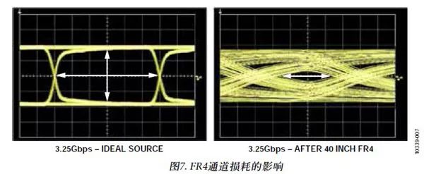
Figure 7 shows the effect of long traces on FR4 material. The left figure shows the ideal eye diagram at the transmitter end. At the receiver end, 40 inches away, the eye diagram is nearly closed, making it difficult for the receiver to recover the data.
Troubleshooting Tips ADC loses the 14th bit
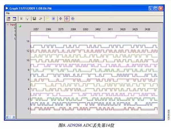
In Figure 8, the VisualAnalog digital display of the data bit indicates that the 14th bit never changed. This may indicate a problem with the device, PCB, or receiver, or that the unsigned data is not large enough to cause the most significant bit to change.
Frequency domain curve when ADC loses the 14th bit
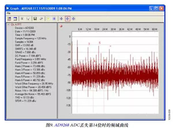
Figure 9 shows the frequency domain view of the above digital data (where the 14th bit did not change). This figure illustrates that the 14th bit is significant, and an error occurred somewhere in the system.
Time domain curve when ADC loses the 14th bit
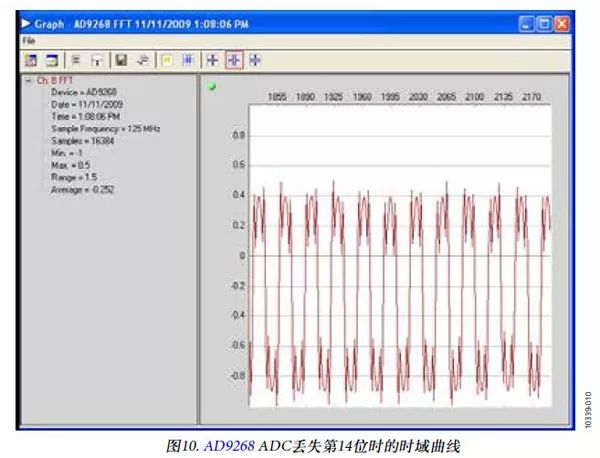
Figure 10 shows the time domain curve of the same data. It is not a smooth sine wave; the data is offset, and there are distinct spikes at multiple points in the waveform.
ADC’s 9th and 10th bits are shorted together
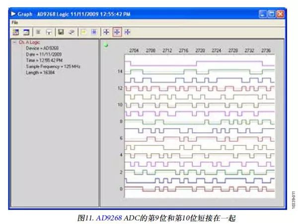
Figure 11 shows that this is no longer a case of losing a bit, but rather two bits being shorted together, so the receiver always receives the same data for these two pins.
Frequency domain curve when ADC’s 9th and 10th bits are shorted together
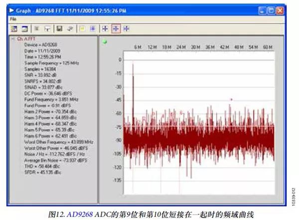
Figure 12 shows the frequency domain view when two bits are shorted together. Although the fundamental frequency sound is very clear, the noise floor is significantly lower than expected. The degree of noise floor distortion depends on which two bits are shorted.
Time domain curve when ADC’s 9th and 10th bits are shorted together
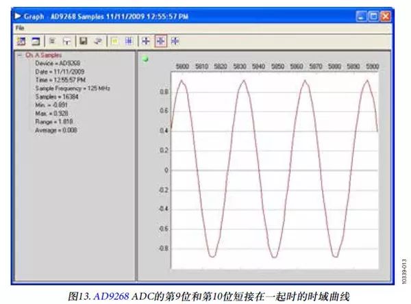
In the time domain graph shown in Figure 13, the problem is relatively subtle. While some smoothness is lost at the peaks and valleys, this is common when the sampling rate approaches the waveform frequency.
Time domain curve when data and clock timing is invalid
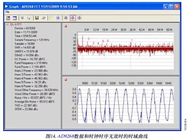
Figure 14 shows a converter situation where timing is invalid due to setup/hold issues. The above errors typically occur in each cycle of the data, while timing errors are not usually persistent. Less severe timing errors may be intermittent. These figures show the time domain and frequency domain curves of data capture that do not meet timing requirements. Note that the time domain errors for each cycle are not consistent. It should also be noted that the noise floor in the FFT/frequency domain is elevated, which often indicates a lost bit, possibly due to timing alignment errors.
Amplified time domain curve when data and clock timing is invalid
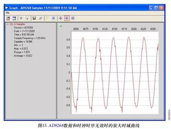
Figure 15 is an enlarged view of the time domain timing error shown in Figure 14. It should also be noted that the errors for each cycle are not consistent, but some errors are repeated. For example, multiple cycles exhibit negative spikes at the troughs of the curves.

Welcome communication engineers and FPGA engineers to follow our official account.

The largest FPGA WeChat technology group in the country
Welcome everyone to join the national FPGA WeChat technology group. This community has tens of thousands of engineers, a group of engineers who love technology, where FPGA engineers help each other and share knowledge, creating a strong technical atmosphere!Quickly invite your friends to join!!

Press and hold to join the national FPGA technology group.
FPGA Home Component City
Advantageous component services, please scan the code to contact the group owner: Jin Juan Email: [email protected] Welcome to recommend to procurement
ACTEL, AD part of the advantageous ordering (operating the full series):

XILINX, ALTERA advantageous spot or ordering (operating the full series):

(The above devices are part of the models, for more models please consult the group owner Jin Juan)
Service concept: FPGA Home Component City aims to facilitate engineers to quickly purchase components, after years of dedicated service, our customer service covers large listed companies, military research units, and small and medium-sized enterprises. Our biggest advantage is emphasizing service first, and achieving fast delivery and favorable prices!
Directly operated brands: Xilinx, ALTERA, ADI, TI, NXP, ST, E2V, Micron, and more than a hundred component brands, especially good at handling components that are banned from the US to China.We welcome engineering friends to recommend us to procurement or consult us personally!We will continue to provide the best service in the industry!

FPGA technology group official thanks to brands: Xilinx, Intel (Altera), Microsemi (Actel), Lattice, Vantis, Quicklogic, Lucent, etc.