The Local Bus, also known as the CPU bus, can be classified into Motorola CPU bus and Intel CPU bus based on the differences in high and low address lines. The ancient CS51 microcontroller is a typical representative of the Intel CPU bus, while the commonly used Power PC is based on the Motorola CPU bus architecture, which evolved from the 60X bus (the 60X bus supports four selectable width modes: 64, 32, 16, and 8 bits). This article uses a Power PC CPU to read and write FPGA internal registers or RAM and handle interrupt responses via the Local Bus as an example to introduce the precautions during the development process.
 In HINOC1.0, the FPGA prototype was interconnected with the Intel XScale PXA270 (ARM CPU) chip using the Local Bus interface timing, which is the same as the timing for the CPU and external asynchronous SRAM interface. Thus, the HINOC chip can be considered as a peripheral of the ARM CPU, allowing the allocation of configurable registers or RAM access space. The specific timing diagram is shown below, with the bus including address, chip select, and read/write signals. The following diagram illustrates a simple read timing. Note that the term asynchronous means that the CPU interface bus and the corresponding FPGA interface are not synchronized, meaning that the signals sent from the CPU to the FPGA do not include a clock signal. The FPGA must sample the address, data, and other signals from the CPU interface using its internal clock signal, and can only use them after synchronization. As shown in the timing diagram for the CPU reading from the FPGA, after the CPU provides the address and read control signal, it must wait for the tAA time before it can read valid data from the data bus. The length of this tAA time can be adjusted by configuring the registers in the PXA270.

 What impressed me deeply was that, when observing the above timing diagram from the FPGA side, one could feel how slow the CPU’s efficiency was. The CPU’s operation of reading and writing to the FPGA internal registers often took dozens of clock cycles, leading to low efficiency. Fortunately, some improved SoC buses like AXI still offer burst modes similar to DMA for continuous read and write operations.
When setting up the simulation environment, the CPU behavior shown in the diagram can be simplified to two simple tasks: read and write (as shown below). The circuit design code on the FPGA side synchronizes the signals sent by the CPU using a two-clock method before decoding the address and passing it to subsequent modules for use.
Currently, this type of bus is used less frequently. However, in many specialized fields, such as aerospace, some domestic CPUs still use similar bus timings. They are simple, reliable, and stable.
What impressed me deeply was that, when observing the above timing diagram from the FPGA side, one could feel how slow the CPU’s efficiency was. The CPU’s operation of reading and writing to the FPGA internal registers often took dozens of clock cycles, leading to low efficiency. Fortunately, some improved SoC buses like AXI still offer burst modes similar to DMA for continuous read and write operations.
When setting up the simulation environment, the CPU behavior shown in the diagram can be simplified to two simple tasks: read and write (as shown below). The circuit design code on the FPGA side synchronizes the signals sent by the CPU using a two-clock method before decoding the address and passing it to subsequent modules for use.
Currently, this type of bus is used less frequently. However, in many specialized fields, such as aerospace, some domestic CPUs still use similar bus timings. They are simple, reliable, and stable.
Debugging Environment Introduction
Hardware Development Board: AX7103; CPU Development Board: p2020; Operating System: Vxworks.
The hardware connection between the CPU and FPGA under the Vxworks operating system is shown in the following diagram 1, using the Local Bus interface.
Figure 1 Hardware Connection Between CPU and FPGA
On the hardware side, the development board does not directly connect to the 50 pins of the p2020 Local Bus. However, on the driver side, it is necessary to develop and test the Local Bus driver. Therefore, a debugging environment needs to be created, utilizing the 68 pins of the AX7103 development board to define the key pins related to the Local Bus (37 pins = 16 pins_addr + 16 pins_data + 3 pins_csn + 1 pin_oen + 1 pin_wen) and interrupt signals to EX_IO1 and EX_IO2. Then, according to the p2020 schematic and matching connectors J5 and J4, the debugging environment is shown in the following diagram 2 (slightly ugly, just for prototype function verification). The figure shows J5 as the p2020 connector (Local Bus related signals); J4 as the p2020 connector (hardwired interrupt, GND signals); EX_IO1 as the Local Bus address, chip select, and read/write enable pins; EX_IO2 as data and interrupt pins.
Note: The voltage levels of the two development boards must be consistent; otherwise, they cannot be directly connected via Dupont wires. It is also recommended that the two development boards share a common ground.
 Figure 2 Actual Debugging Environment of Hardware Board and CPU Board
As previously mentioned, the interfaces used for data interaction between the FPGA and CPU are PCIe and other interfaces. In TSN or TTE systems, PCIe interfaces are often used at endpoints, while Local Bus interfaces are commonly used for data interaction between CPU and FPGA within switches. This article only discusses the debugging process of the Local Bus. For the hardware side, the Local Bus is simpler to develop compared to PCI and PCIe, as it only requires completing the mapping of CPU memory addresses to hardware registers and RAM addresses, as well as the timing of the read/write enable signals and chip select signals. This Local Bus development involves establishing a Local Bus test project on the hardware side, in conjunction with debugging the register read/write functionality and interrupt functionality of the Local Bus driver.
2.1.Data Read/Write Operations
Regarding the register read/write functionality, a valuable reference for the introduction of the Local Bus is this link: https://wenku.baidu.com/view/aeca83593b3567ec102d8a80.html?from=search. Since the Local Bus is simple, there is not much to introduce. The theoretical part can be found in the link. Here, I will attach the timing diagrams of the key signals for read/write operations, as shown in diagrams 3 and 4. The same Local Bus interface may have some inconsistencies in address and data widths across different CPU processors. For example, in the BM3803 processor, the address data lines are not multiplexed, and the data width is 32 bits (double-word operation); in the p2020 processor, the data line LAD is multiplexed (the LALE signal latches the high 11 bits of the address, and if only a 16-bit address is used, LALE can be left unconnected), with a data width of 16 bits (byte operation).
2.2.Interrupt Functionality
For interrupts, traditional hardwired interrupts are used. According to the p2020 schematic, apart from irq3, which is already occupied, there are six other hardwired interrupts (irq0/1/2/4/5/6) available for peripherals, all located at the J4 connector. From the p2020 Datasheet, it can be seen that there are 64 types of internal interrupts and 12 types of external interrupts. For our debugging, we are using the external interrupt irq1.
3.1.Data Read/Write Operations
At the beginning of debugging, it can be seen from the p2020 schematic that CS0 and CS1 are used for the internal nand_flash and nor_flash, respectively. Additionally, three output chip select signals (CS2, CS3, and CS4) indicate that up to eight Local Bus peripherals can be connected. These peripherals (including *_flash) share data lines, address lines, and read/write enables. The first step is to determine which chip select signal is used by the driver. The driver is also explored, and the driver code indicates that only CS4 is used, while CS2 is masked in the original routine. By capturing cpu_csn[2:0] on the hardware side, it is found that cpu_csn[0] also has a low chip select state. After modifying the driver, CS2 is retained, so that every read/write operation by the driver can trigger “cpu_csn[2:0]==3’b110”. When the CPU board performs read/write operations on the address range 0xf1000_0000~0xf1000_ffff (128KB), it will pull down CS2, which corresponds to reading/writing to registers/RAM on the hardware side.
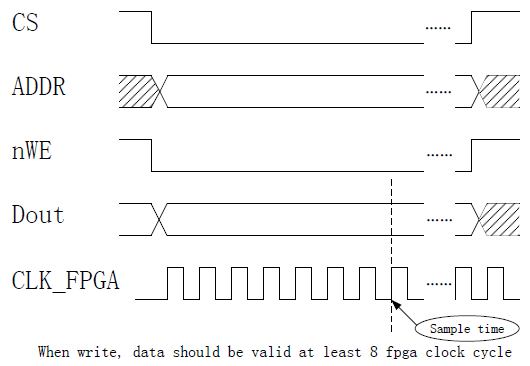
Testing the write function, after the CPU starts, the driver will write 16’h5555 to memory address 0xf100_0118, as shown in diagram 5. First, the write address is given, then the chip select signal is pulled low, almost simultaneously pulling down the write enable signal, allowing data to be written from the CPU to the FPGA.
Figure 2 Actual Debugging Environment of Hardware Board and CPU Board
As previously mentioned, the interfaces used for data interaction between the FPGA and CPU are PCIe and other interfaces. In TSN or TTE systems, PCIe interfaces are often used at endpoints, while Local Bus interfaces are commonly used for data interaction between CPU and FPGA within switches. This article only discusses the debugging process of the Local Bus. For the hardware side, the Local Bus is simpler to develop compared to PCI and PCIe, as it only requires completing the mapping of CPU memory addresses to hardware registers and RAM addresses, as well as the timing of the read/write enable signals and chip select signals. This Local Bus development involves establishing a Local Bus test project on the hardware side, in conjunction with debugging the register read/write functionality and interrupt functionality of the Local Bus driver.
2.1.Data Read/Write Operations
Regarding the register read/write functionality, a valuable reference for the introduction of the Local Bus is this link: https://wenku.baidu.com/view/aeca83593b3567ec102d8a80.html?from=search. Since the Local Bus is simple, there is not much to introduce. The theoretical part can be found in the link. Here, I will attach the timing diagrams of the key signals for read/write operations, as shown in diagrams 3 and 4. The same Local Bus interface may have some inconsistencies in address and data widths across different CPU processors. For example, in the BM3803 processor, the address data lines are not multiplexed, and the data width is 32 bits (double-word operation); in the p2020 processor, the data line LAD is multiplexed (the LALE signal latches the high 11 bits of the address, and if only a 16-bit address is used, LALE can be left unconnected), with a data width of 16 bits (byte operation).
2.2.Interrupt Functionality
For interrupts, traditional hardwired interrupts are used. According to the p2020 schematic, apart from irq3, which is already occupied, there are six other hardwired interrupts (irq0/1/2/4/5/6) available for peripherals, all located at the J4 connector. From the p2020 Datasheet, it can be seen that there are 64 types of internal interrupts and 12 types of external interrupts. For our debugging, we are using the external interrupt irq1.
3.1.Data Read/Write Operations
At the beginning of debugging, it can be seen from the p2020 schematic that CS0 and CS1 are used for the internal nand_flash and nor_flash, respectively. Additionally, three output chip select signals (CS2, CS3, and CS4) indicate that up to eight Local Bus peripherals can be connected. These peripherals (including *_flash) share data lines, address lines, and read/write enables. The first step is to determine which chip select signal is used by the driver. The driver is also explored, and the driver code indicates that only CS4 is used, while CS2 is masked in the original routine. By capturing cpu_csn[2:0] on the hardware side, it is found that cpu_csn[0] also has a low chip select state. After modifying the driver, CS2 is retained, so that every read/write operation by the driver can trigger “cpu_csn[2:0]==3’b110”. When the CPU board performs read/write operations on the address range 0xf1000_0000~0xf1000_ffff (128KB), it will pull down CS2, which corresponds to reading/writing to registers/RAM on the hardware side.
Testing the write function, after the CPU starts, the driver will write 16’h5555 to memory address 0xf100_0118, as shown in diagram 5. First, the write address is given, then the chip select signal is pulled low, almost simultaneously pulling down the write enable signal, allowing data to be written from the CPU to the FPGA.
 Figure 5 Board-Level Write Operation
In comparison to the simplicity of the write operation, problems arose during the read operation. We also connected the read enable lines of AX7103 and p2020 properly (address, data, and chip select signals were connected first), but found that the CPU could not start. However, when this signal was connected to the unused EX_IO, the CPU could start normally, indicating that the read enable signal interfered with the CPU’s startup. However, the attributes of cpu_oen and cpu_wen are the same; input to the FPGA does not output to the CPU and cause it not to start. Upon reviewing the p2020 datasheet, it was found that the LGPL2 signal on the p2020 has dual definitions:
1. Read enable for the Local Bus cpu_oen;
2. Configuring the e500 core pll clock duty cycle in conjunction with LBCTL and LALE signals.
It was suspected that the level of cpu_oen on the FPGA side briefly affected the LGPL2 of the CPU side after the system started. Therefore, we changed the read enable to an inout signal, keeping it in high impedance state for 10 seconds after the CPU starts, serving as isolation. After 10 seconds, the p2020 bootrom would be loaded and could boot up, but the actual test results showed that the CPU still could not start normally.
We completely disconnected all Dupont wires, leaving only the connection of the read enable wire, and found that the CPU could start normally. This indicated that the level of the read enable on the FPGA side did not affect the startup of the CPU. To specifically locate which signal was causing the issue, we reconnected the wires one by one. Finally, after connecting the read enable line, write enable line, chip select line, and address line, the CPU board could boot up normally, and the FPGA could capture the correct read/write timing (though the read/write data was not visible). After inserting the data line, the CPU could not start. Thus, we finally located the problem. For this, the FPGA side made its first modification, implementing a simple delay process where the data line remained in high impedance for 20 seconds (during which the CPU could perform Local Bus write operations), and only after booting up would the data be enabled for reading. This approach is somewhat clumsy but indeed resolves the issue of the CPU not starting normally; it is a temporary fix but not a fundamental solution, after all, deliberate delays are unreliable.
/**********First Modification********/
//rst_done only becomes 1 after 20 seconds, before which cpu_data remains high impedance
assign cpu_data =((cpu_oen==1’b0)&& (rst_done==1’b1)) ? cpu_rdata : 16’bz;
assign cpu_wdata = cpu_data ;
/*******************************/
Suddenly inspired… By adding an additional constraint condition “(rst_done==1’b1)” to the line “assign cpu_data =(cpu_oen==1’b0) ? cpu_rdata : 16’bz;” it allowed the CPU to start, indicating that at the beginning of the CPU startup, the low enable of cpu_oen caused cpu_data to output interference to the CPU side’s data line. As mentioned at the beginning of this article, the p2020 also has nand_flash and nor_flash, and during the p2020 startup, it needs to read and write data from these flashes, which also pulls down cpu_oen. At this time, the Local Bus reads the default value 16’h0, while some useful values should have been read from *_flash and are overwritten by 16’h0. To verify this guess, I made a second modification to the data signal code.
/**********Second Modification********/
//The CPU will only output cpu_rdata after the localbus is selected with CS_4, otherwise it remains high impedance.
assign cpu_data =((cpu_oen==1’b0)&& (cpu_csn[2]==1’b0)) ? cpu_rdata : 16’bz;
assign cpu_wdata = cpu_data ;
/*******************************/
After this modification, the CPU started normally because when the p2020 started, it would read from *_flash. Although cpu_oen was pulled low, the chip select was not CS2. Therefore, at this time, the FPGA’s cpu_data remained high impedance until the chip select was successful and the read enable was low effective, allowing the read data to be output. Ultimately, the correct board-level read operation timing is shown in diagram 6.
Figure 5 Board-Level Write Operation
In comparison to the simplicity of the write operation, problems arose during the read operation. We also connected the read enable lines of AX7103 and p2020 properly (address, data, and chip select signals were connected first), but found that the CPU could not start. However, when this signal was connected to the unused EX_IO, the CPU could start normally, indicating that the read enable signal interfered with the CPU’s startup. However, the attributes of cpu_oen and cpu_wen are the same; input to the FPGA does not output to the CPU and cause it not to start. Upon reviewing the p2020 datasheet, it was found that the LGPL2 signal on the p2020 has dual definitions:
1. Read enable for the Local Bus cpu_oen;
2. Configuring the e500 core pll clock duty cycle in conjunction with LBCTL and LALE signals.
It was suspected that the level of cpu_oen on the FPGA side briefly affected the LGPL2 of the CPU side after the system started. Therefore, we changed the read enable to an inout signal, keeping it in high impedance state for 10 seconds after the CPU starts, serving as isolation. After 10 seconds, the p2020 bootrom would be loaded and could boot up, but the actual test results showed that the CPU still could not start normally.
We completely disconnected all Dupont wires, leaving only the connection of the read enable wire, and found that the CPU could start normally. This indicated that the level of the read enable on the FPGA side did not affect the startup of the CPU. To specifically locate which signal was causing the issue, we reconnected the wires one by one. Finally, after connecting the read enable line, write enable line, chip select line, and address line, the CPU board could boot up normally, and the FPGA could capture the correct read/write timing (though the read/write data was not visible). After inserting the data line, the CPU could not start. Thus, we finally located the problem. For this, the FPGA side made its first modification, implementing a simple delay process where the data line remained in high impedance for 20 seconds (during which the CPU could perform Local Bus write operations), and only after booting up would the data be enabled for reading. This approach is somewhat clumsy but indeed resolves the issue of the CPU not starting normally; it is a temporary fix but not a fundamental solution, after all, deliberate delays are unreliable.
/**********First Modification********/
//rst_done only becomes 1 after 20 seconds, before which cpu_data remains high impedance
assign cpu_data =((cpu_oen==1’b0)&& (rst_done==1’b1)) ? cpu_rdata : 16’bz;
assign cpu_wdata = cpu_data ;
/*******************************/
Suddenly inspired… By adding an additional constraint condition “(rst_done==1’b1)” to the line “assign cpu_data =(cpu_oen==1’b0) ? cpu_rdata : 16’bz;” it allowed the CPU to start, indicating that at the beginning of the CPU startup, the low enable of cpu_oen caused cpu_data to output interference to the CPU side’s data line. As mentioned at the beginning of this article, the p2020 also has nand_flash and nor_flash, and during the p2020 startup, it needs to read and write data from these flashes, which also pulls down cpu_oen. At this time, the Local Bus reads the default value 16’h0, while some useful values should have been read from *_flash and are overwritten by 16’h0. To verify this guess, I made a second modification to the data signal code.
/**********Second Modification********/
//The CPU will only output cpu_rdata after the localbus is selected with CS_4, otherwise it remains high impedance.
assign cpu_data =((cpu_oen==1’b0)&& (cpu_csn[2]==1’b0)) ? cpu_rdata : 16’bz;
assign cpu_wdata = cpu_data ;
/*******************************/
After this modification, the CPU started normally because when the p2020 started, it would read from *_flash. Although cpu_oen was pulled low, the chip select was not CS2. Therefore, at this time, the FPGA’s cpu_data remained high impedance until the chip select was successful and the read enable was low effective, allowing the read data to be output. Ultimately, the correct board-level read operation timing is shown in diagram 6.
 Figure 6 Board-Level Read Operation
The p2020 processor’s interrupts are divided into external and internal interrupts. We are using external interrupt 1. Under Vxworks, the external interrupt vector starts numbering from 0, so the vector assigned to external interrupt 1 is 1. First, the interrupt vector is bound to the device in the BSP and registered in the hcfDevice device list. Then, in the driver, the interrupt is initialized and enabled, allowing it to receive interrupt signals from the external interrupt 1 pin.
It should be noted that the following diagram 7 describes the irq of the p2020 datasheet: high state generates an interrupt, while low state does not generate an interrupt. However, actual board-level testing found that irq is effective when low, generating a hardwired interrupt.
Figure 6 Board-Level Read Operation
The p2020 processor’s interrupts are divided into external and internal interrupts. We are using external interrupt 1. Under Vxworks, the external interrupt vector starts numbering from 0, so the vector assigned to external interrupt 1 is 1. First, the interrupt vector is bound to the device in the BSP and registered in the hcfDevice device list. Then, in the driver, the interrupt is initialized and enabled, allowing it to receive interrupt signals from the external interrupt 1 pin.
It should be noted that the following diagram 7 describes the irq of the p2020 datasheet: high state generates an interrupt, while low state does not generate an interrupt. However, actual board-level testing found that irq is effective when low, generating a hardwired interrupt.
 Figure 7 p2020 Interrupt irq Description
When the driver receives an interrupt, it needs to reset the hardwired interrupt. Referring to the PCIe bus INTa interrupt operation (here’s the key! The minimum time interval for VxWorks to respond to PCIe interrupts was tested), we define the 0x110 register as the interrupt register. When the driver writes 1 to the [15] bit of 0x110 and then writes 0, the hardware will pull the hardwired interrupt signal back to a high level reset state. The interrupt timing is shown in the following diagram 8.
Figure 7 p2020 Interrupt irq Description
When the driver receives an interrupt, it needs to reset the hardwired interrupt. Referring to the PCIe bus INTa interrupt operation (here’s the key! The minimum time interval for VxWorks to respond to PCIe interrupts was tested), we define the 0x110 register as the interrupt register. When the driver writes 1 to the [15] bit of 0x110 and then writes 0, the hardware will pull the hardwired interrupt signal back to a high level reset state. The interrupt timing is shown in the following diagram 8.
 Figure 8 Interrupt Timing
【Free】 FPGA Engineer Recruitment Platform
FPGA Chip Industry Popular Science
SANXIN-B01 Development Board Verilog Tutorial V3 Electronic Edition
Job Interview | Latest Summary of FPGA or IC Interview Questions
FPGA Zero-Basis Learning: Image Display System Design
Project Cooperation | Announcement for Undertaking FPGA Projects
FPGA Timing Analysis and Constraints Special Course, covering Quartus, ISE, and Vivado, can be enrolled online at any time!
FPGA Image Processing Special Course, covering Quartus, ISE, and Vivado, can be enrolled online at any time!
FPGA Employment Class, starting on 2023.02.08, rich course content, systematic learning of FPGA, high-paying employment, online and offline synchronization!

FPGA Technology Jianghu Wide Release Jianghu Post
No ads, pure mode, providing a clean space for technical exchanges, from novice to industry elite and industry leaders, covering various directions from military to civilian enterprises, from communication, image processing to artificial intelligence, QQ WeChat dual selection, FPGA technology Jianghu creates the purest and most professional technical exchange learning platform.
FPGA Technology Jianghu WeChat Group

Add the group owner’s WeChat, note your name + company/school + position/major to join the group
FPGA Technology Jianghu QQ Group

Note: Join the group with your name + company/school + position/major