Yangzhou Lattice Semiconductor specializes in providing high-purity, large-size single crystal silicon & polycrystalline silicon materials, and can perform deep processing customization such as cutting, grinding, polishing, and drilling, including silicon wafers, silicon components, silicon target materials, silicon seed crystals, silicon electrodes, silicon rings, silicon window pieces, and other silicon products.
The etching technique is a method in semiconductor technology that selectively etches or removes the surface of a semiconductor substrate or the thin film covering it according to the mask pattern or design requirements. Etching technology is not only a fundamental manufacturing process for semiconductor devices and integrated circuits but is also applied in the processing of thin-film circuits, printed circuits, and other micro-patterns. Etching can be divided into wet etching and dry etching.
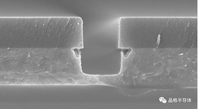
The mechanism of etching can be roughly divided into processes such as “reactants approaching the surface”, “surface oxidation”, “surface reaction”, and “products leaving the surface”. Therefore, the entire etching process includes the diffusion effects of reactants approaching and products leaving, as well as the chemical reaction. The total etching time is the sum of the time spent on diffusion and chemical reaction. Whichever takes longer will determine the speed of the entire etching process, hence the distinction between “reaction limited” and “diffusion limited” etching.
Currently, the dry etching market accounts for 90%, while wet etching accounts for 10%. Wet etching is generally suitable for larger sizes (greater than 3 microns) and is used to etch certain layers on silicon wafers or to remove residues after dry etching. The majority of production uses dry etching. Dry etching and wet etching processes utilize different principles of chemical treatment. In dry etching, both chemical and physical reactions occur when etching the surface material. Therefore, the etching characteristics exhibit both chemical isotropy and physical anisotropy. Isotropy refers to etching occurring in both horizontal and vertical directions, while anisotropy refers to etching occurring in a single vertical direction. Dry etching is used for high-precision pattern transfer. Currently, China’s etching processes and equipment have reached a relatively advanced level compared to photolithography, achieving high etching selectivity, better dimensional control, low aspect ratio dependence etching, and lower plasma damage.Etching SelectivityEtching selectivity (Etch Selectivity) describes the ratio of etching rates between the desired material and the material that should not be etched during the etching process. Etching selectivity can describe the relative etching rates between the mask and the target material, or the relative etching rates between different material layers. If a target material is etched at a speed 10 times that of the mask or substrate material, then the etching selectivity is 10:1.
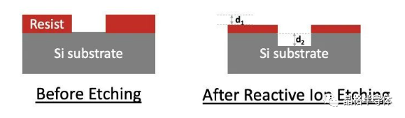
The higher the etching selectivity, the faster the target material is etched, while the etching rate of the mask or adjacent layers is very slow. High etching selectivity ensures that the mask is almost not consumed during the etching process, and that the reaction stops after the target material is etched, preventing further etching of adjacent layers. Generally, a selectivity of >5:1 is considered high selectivity. In some cases, selectivity can be as high as 100:1.The lower the etching selectivity, the more similar the etching rates of the two materials. When selectivity is low, the mask will not provide as much protection for the target material as desired. This means that a thicker mask must be used to etch to the required depth, which increases the difficulty and cost of mask fabrication. On the other hand, when the target material is completely etched, the underlying material will still be etched, which is undesirable.
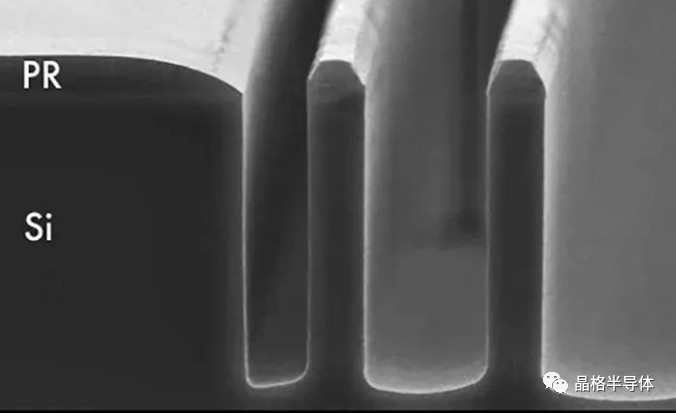
Considerations in the Dry Etching Process
- Maintain Uniformity. Uniformity refers to how similar the etching rates are across different parts of the wafer. During the process, the etching rates at different parts of the wafer may vary over time, leading to different shapes, which may cause defects or changes in characteristics in chips located in certain areas.
- Etch Rate.It indicates how much film can be removed in a given time.Etch rate mainly depends on the number of reactive atoms and ions required for the surface reaction and the energy of the ions, so improving control over these factors can enhance overall yield.Additionally, selectivity, profile, and other factors are also important in dry etching.
Yangzhou Lattice Semiconductor specializes in providing high-purity, large-size single crystal silicon & polycrystalline silicon materials, and can perform deep processing customization such as cutting, grinding, polishing, and drilling, including silicon wafers, silicon components, silicon target materials, silicon seed crystals, silicon electrodes, silicon rings, silicon window pieces, and other silicon products.