
1. Introduction to PCB Materials(1) Concept, Function, and Background of Printed Circuit Boards1. The English term for printed circuit board: Printed Circuit Board2. The abbreviation for printed circuit board: PCB3. The main functions of printed circuit boards: to support circuit components and interconnect circuit components, namely the two main roles of support and interconnection.4. PCBs were born in the 1940s and 1950s and developed in the 1980s and 1990s. With the advancement of semiconductor technology and computer technology, printed circuit boards have evolved towards high density, fine lines, and more layers, and their design technology has progressed from initial manual drawing to computer-aided design (CAD) and electronic design automation (EDA).(2) Classification of PCBs (Copper Clad Laminates)Definition of copper clad laminatea. Copper clad laminate: abbreviated as CCL, it is the most basic material for making circuit boards, consisting of a layer or two layers of laminated board covered with metal copper foil.b. Copper clad laminates are classified into rigid and flexible types.c. The substrate of copper clad laminate is a non-conductive insulating material.d. Copper clad laminate is a laminated product formed by copper foil/bonding resin/paper or fiber cloth under heat and pressure.(2) Classification of PCBs (Copper Clad Laminates) – Single-Sided Boards1. Paper-based phenolic resin – paper board:a. Composition characteristics: made from paper scraps and phenolic resin, appearing flat like paper on the surface.b. Includes: FR-1, FR-2, FR-3, XBC, HB(Currently, TPV mostly uses FR-1/FR-2; FR-1 is often used for MNT, while FR-2 is more commonly used for TVs. FR-2 has higher electrical performance requirements and is more expensive than FR-1, but other performance differences are minimal).c. Advantages: low raw material cost, and due to its softer texture, it can be punched, resulting in lower processing costs during the circuit board manufacturing process.d. Relatively poor hardness, easily absorbs moisture in humid environments, and experiences significant thermal expansion and contraction changes at high temperatures, with electrical performance lower than that of fiber boards. (Example: easily deforms during wave soldering).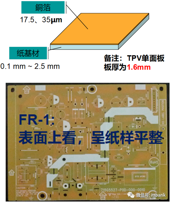 2. Paper-based epoxy resin – composite fiber board:a. Composition characteristics: the substrate is made from paper scraps mixed with epoxy resin, with a glass fiber surface, pressed together, appearing textured on the surface.b. Includes: CEM-1 (paper core), CEM-3 (glass fiber core). (Currently, TPV mostly uses CEM-1)CEM-1 composition: copper foil + paper (core) + epoxy resin (core) + glass fiber cloth (surface)CEM-3 composition: copper foil + glass fiber non-woven fabric (core) + epoxy resin (core) + glass fiber cloth (surface)CEM-3 contains more fiber layers than CEM-1, thus its flame resistance, insulation, hardness, etc., are superior to CEM-1, and it can be used to replace FR-4 for some double-sided and multilayer boards.c. Advantages: composite fiber boards are cheaper than glass fiber boards, solving the hardness issues of paper boards and the difficulty of punching fiber boards.d. Disadvantages: although the electrical performance is close to that of glass fiber boards, it cannot completely replace FR-4 materials; only some less demanding circuit boards can use this material as a substitute for FR-4.
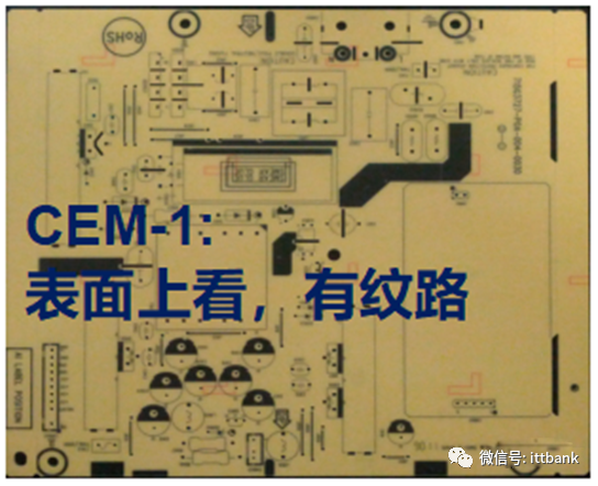 (2) Classification of PCBs (Copper Clad Laminates) – Double-Sided Boards, Multilayer Boards1. Glass fiber cloth-based epoxy resin – glass fiber board:a. Composition characteristics: the substrate is made from glass fiber cloth mixed with epoxy resin, with a glass fiber cloth surface, pressed together, appearing textured on the surface, and when viewed from the side, it has fiber strands and appears layered.b. Includes: FR-4, etc. (Currently, TPV uses FR-4 for both double-sided and multilayer boards).c. Advantages: high strength, heat and fire resistance (will not burn), corrosion resistance (not easily corroded or moldy), moisture resistance, thermal properties (low expansion coefficient, high thermal conductivity), electrical properties (non-conductive, insulating).d. Disadvantages: high cost, high manufacturing process requirements (e.g., cannot be punched).
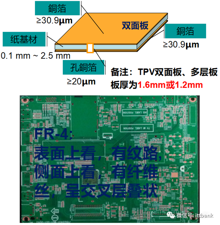 2. Ceramic and metal materials: such as iron-based, aluminum-based, copper-based, mainly used in military and aerospace fields.(2) Classification of PCBs (Copper Clad Laminates) – Material IdentificationPCB material coding rule No. 34:
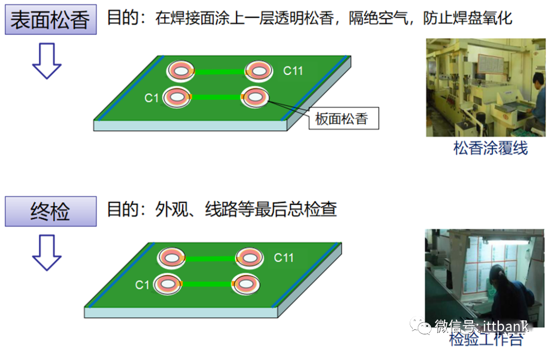
 Special requirement code third digit represents the material used: 1 – FR-1; 2 – FR-2; 3 – CEM-1; 4 – FR-4 double-sided board; 5 – FR-4 four-layer board; 6 – FR-4 six-layer board; 7 – FPC (flexible board)Example: 715G5713-M01-000-005K Material used: FR-4 four-layer board(2) Classification of PCBs (Copper Clad Laminates) – Surface Treatment1. OSP Process: OSP stands for Organic Solderability Preservative, and its process principle is to form a uniform, extremely thin, transparent organic coating on the solder pads and through holes of the circuit board through a chemical reaction between an imidazole-derived active component and the surface of the metal copper. This coating has excellent heat resistance, with a typical thickness of 0.2-0.5μm.(Currently, TPV requires OSP thickness to meet the requirements for two reflow soldering and one wave soldering. Manufacturers can achieve 0.2~0.35μm) During soldering, the protective film decomposes, evaporates, and melts into the solder paste or acidic flux, exposing the copper surface, allowing the solder to react with clean copper. Due to its low production cost and mature technology, it is now widely used.(2) Classification of PCBs (Copper Clad Laminates) – Surface Treatment2. Advantages and Disadvantages of OSP Process and Applicationsa. Advantages: flat, cheap, OSP is only attracted to the copper surface and has no affinity for other surfaces such as solder mask layers, so it does not adhere to their surfaces, making it widely applicable.b. Disadvantages: ① Short shelf life, under vacuum packaging conditions, the shelf life is 3 months. During storage, it should not come into contact with acidic substances, and the temperature should not be too high, otherwise, it will evaporate.② Difficult to detect, colorless and transparent.③ OSP itself is insulating; imidazole-based OSP, which forms a thicker coating layer, will affect electrical testing and cannot be used as a coating on electrical contact surfaces such as gold fingers, keyboard keys, test points, etc.④ Cannot be subjected to multiple reflow soldering, generally limited to 3 times, and needs to be considered during double-sided reflow soldering and repair. After several generations of improvements, its heat resistance, storage life, and compatibility with flux have greatly improved.⑤ Soldering temperature is relatively increased to 225°C, and during soldering, a stronger (acidic component) flux must be added to eliminate the protective film, otherwise, it will lead to soldering defects.2. Overview of PCB Production Process
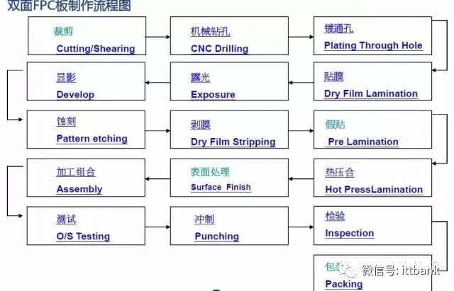
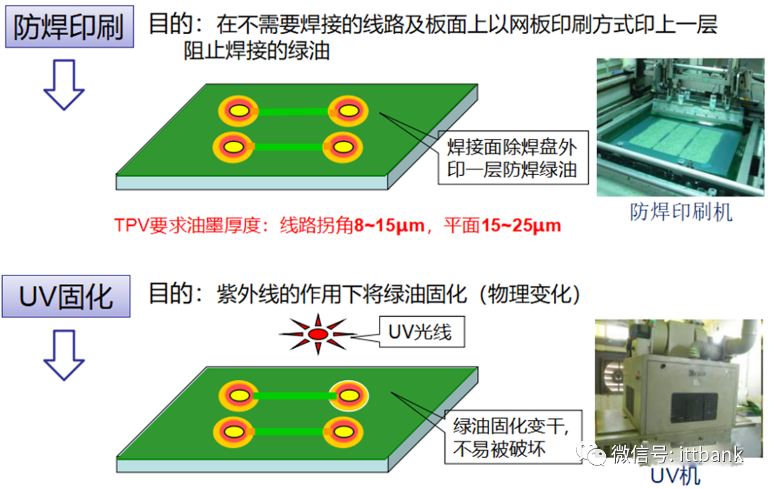
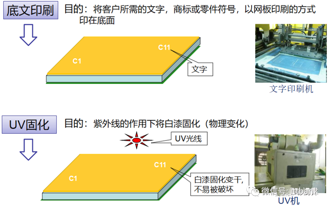
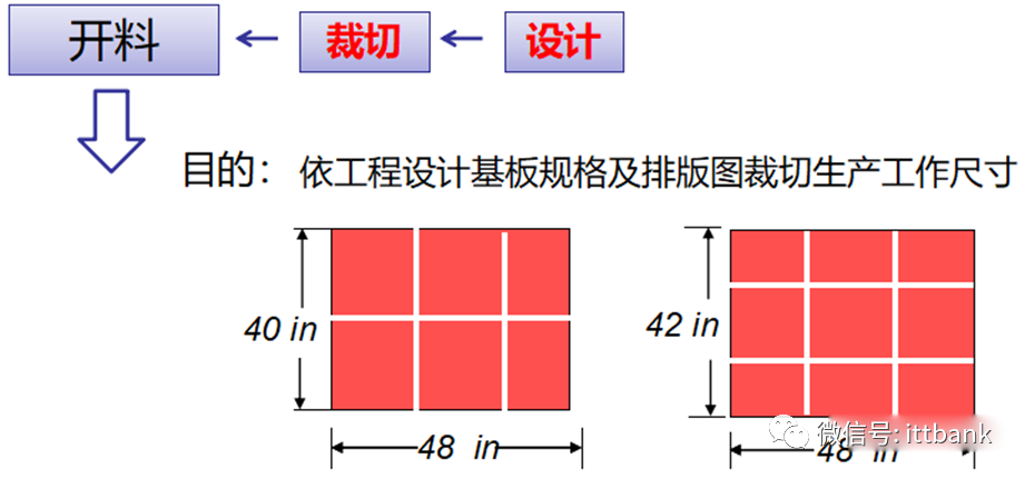
 (1) Single-Sided Board Production Process
 Overview of PCB Production Process – Single-Sided Board
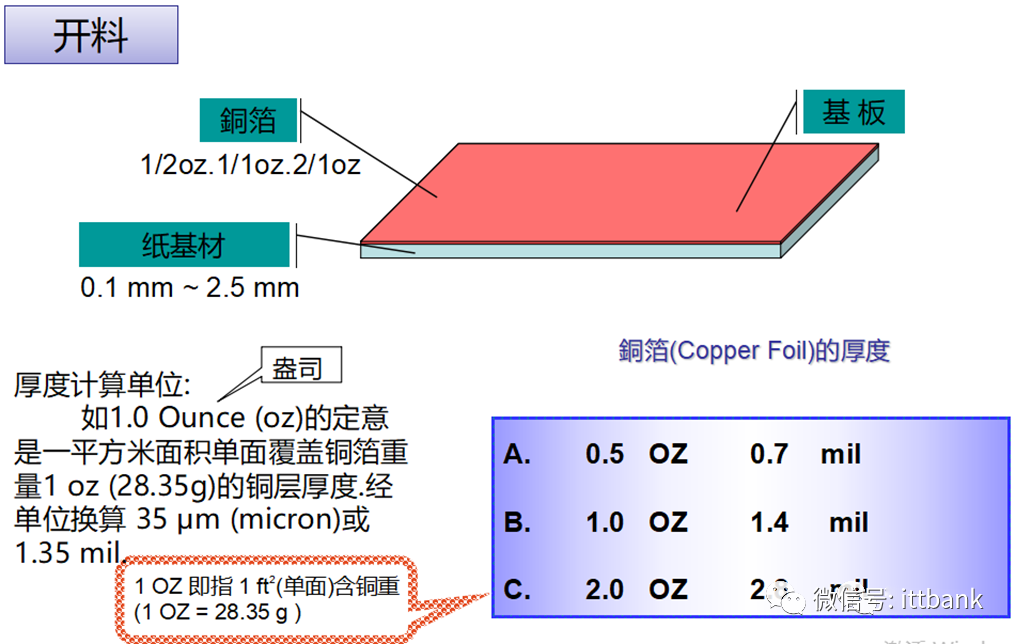
 Materials used:FR1—paper-based boardCEM-1–composite fiber board, also known as semi-glass fiber board
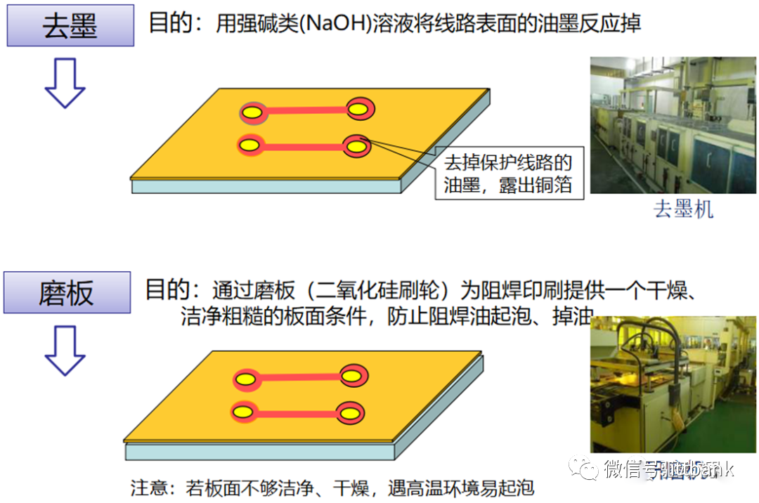
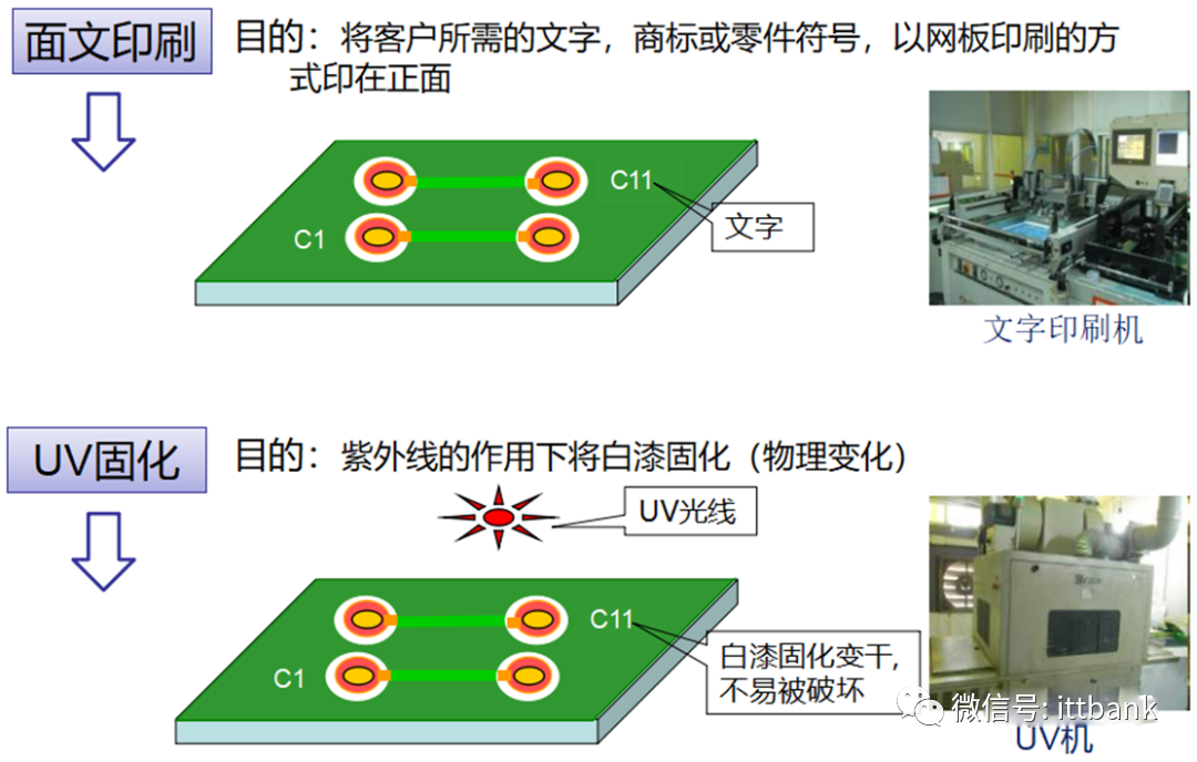
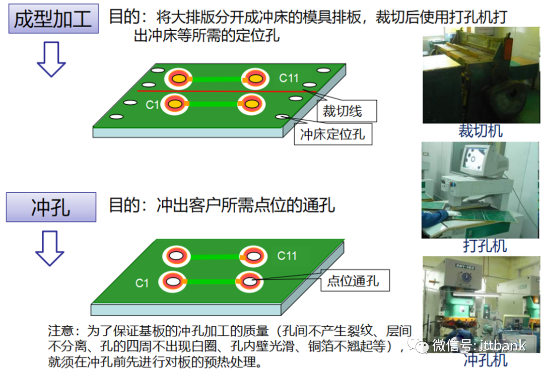
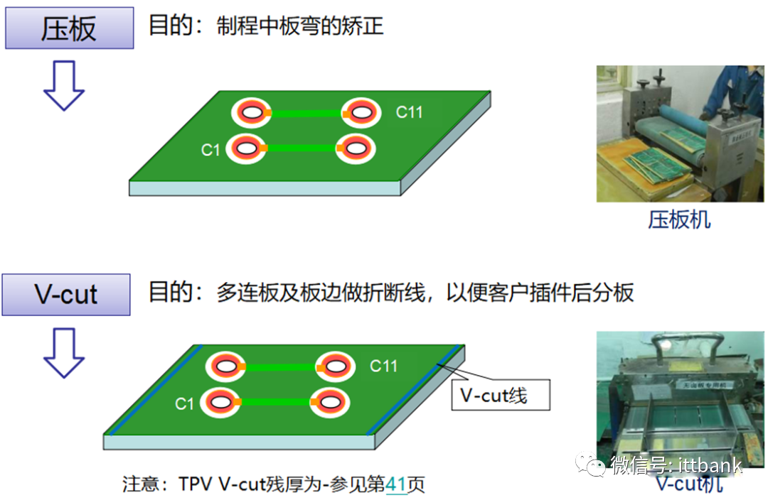
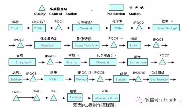
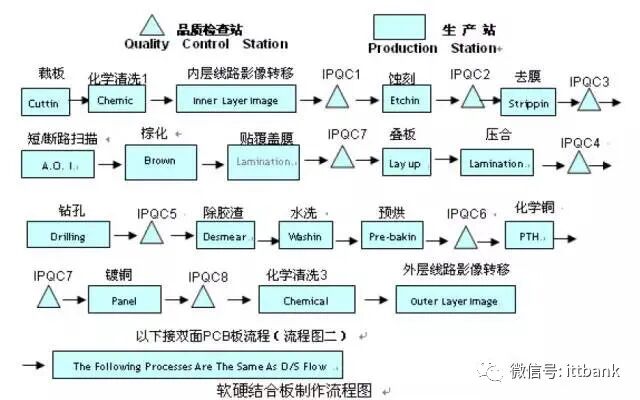
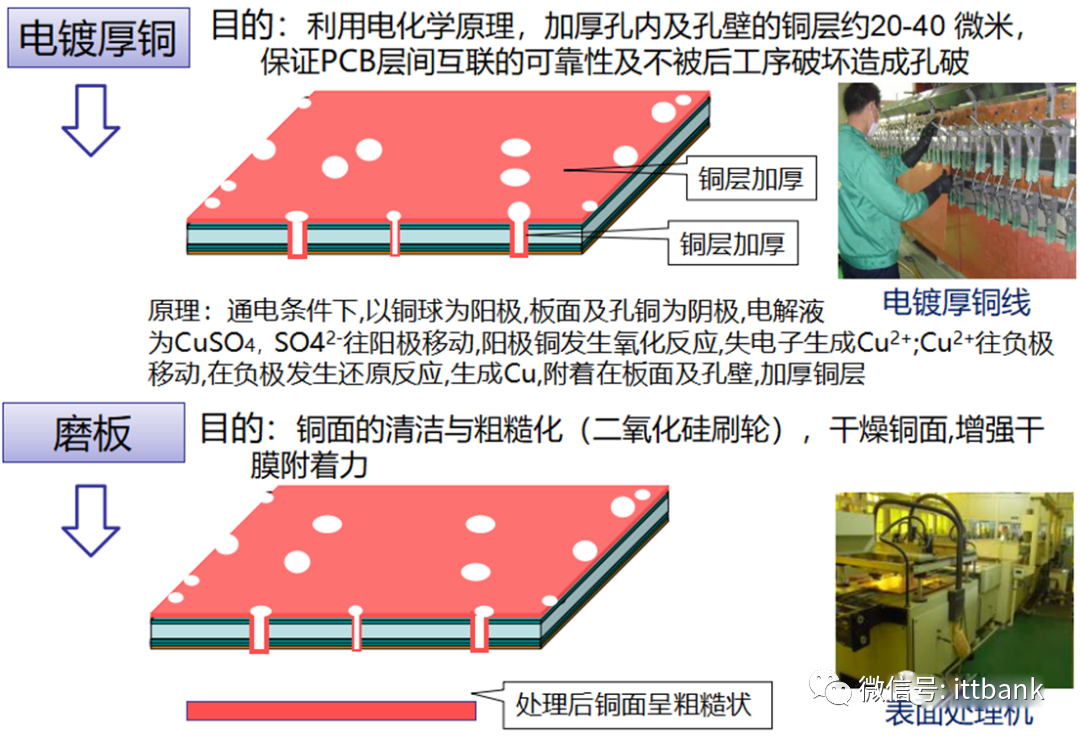
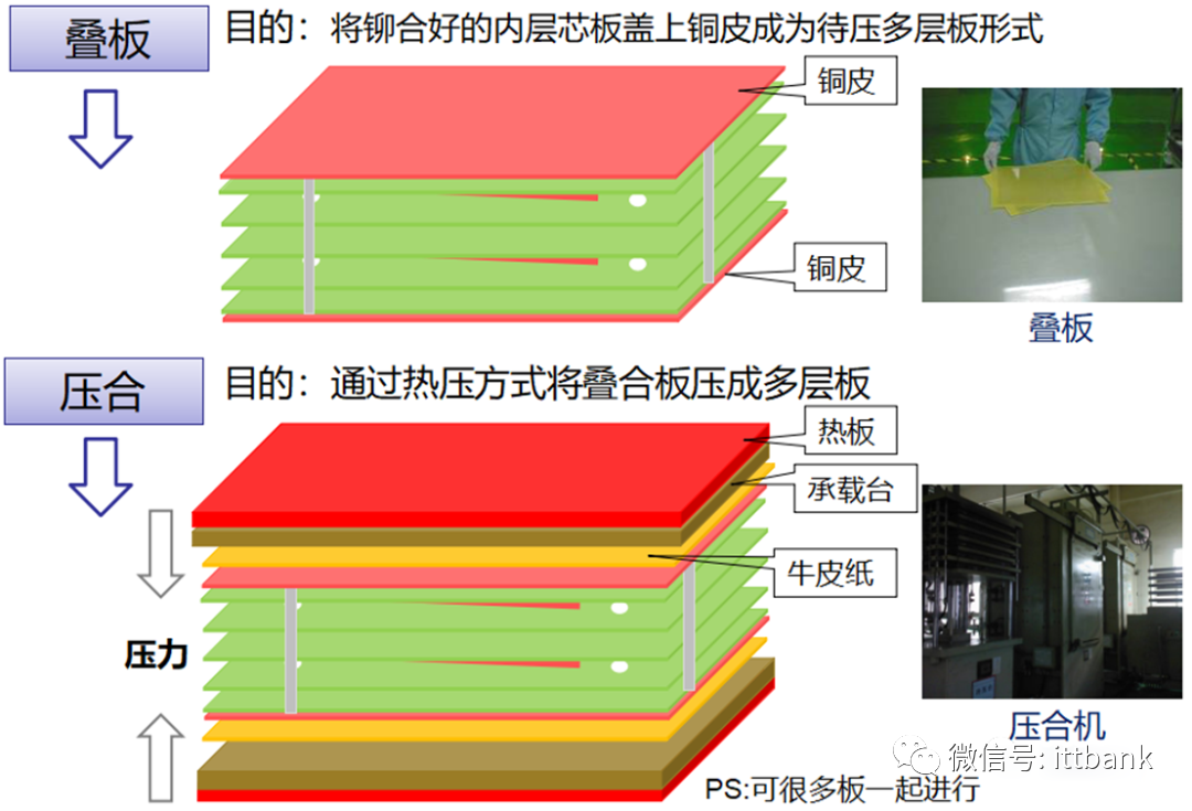
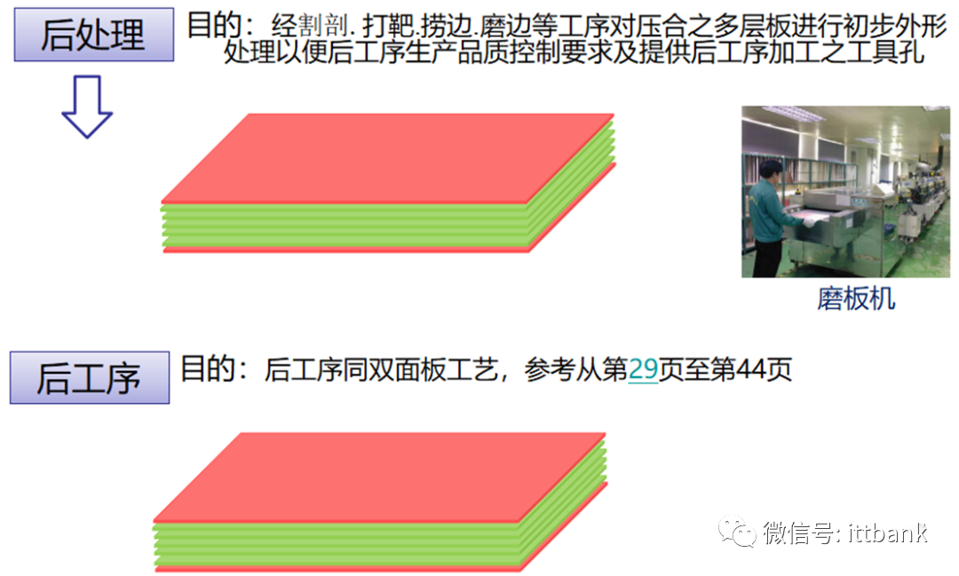
 (2) Double-Sided Board Production Process
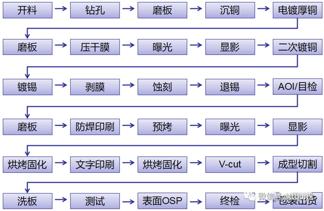 Overview of PCB Production Process – Double-Sided Board
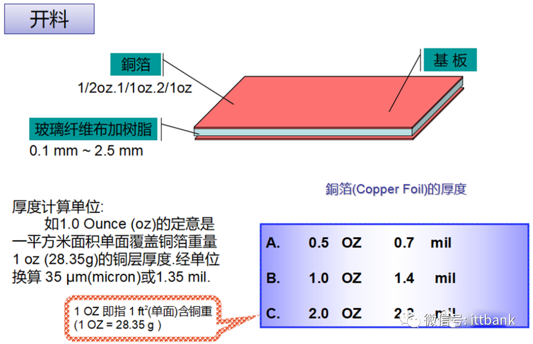
 Materials used:FR4—glass cloth-based board
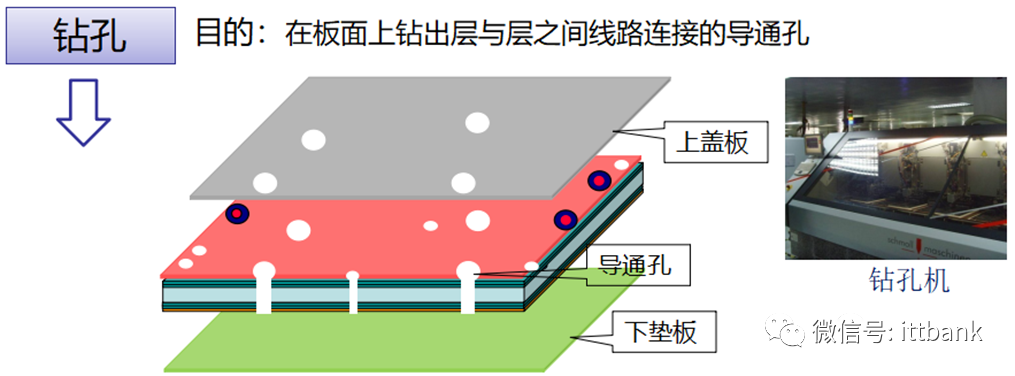 Cover plate (aluminum plate): prevents burrs from drilling; protects the copper foil layer from being damaged; improves hole position accuracy; cools the drill bit, reducing drilling temperature. Thickness: 0.15-0.2mm.Backing plate (composite plate): protects the drilling machine table during the process; prevents burrs; reduces drill bit temperature and cleans drill bit grooves from glue residue.Drill bit: made from tungsten carbide, cobalt, and organic adhesive.TPV requires hole wall roughness to be ≤25μm
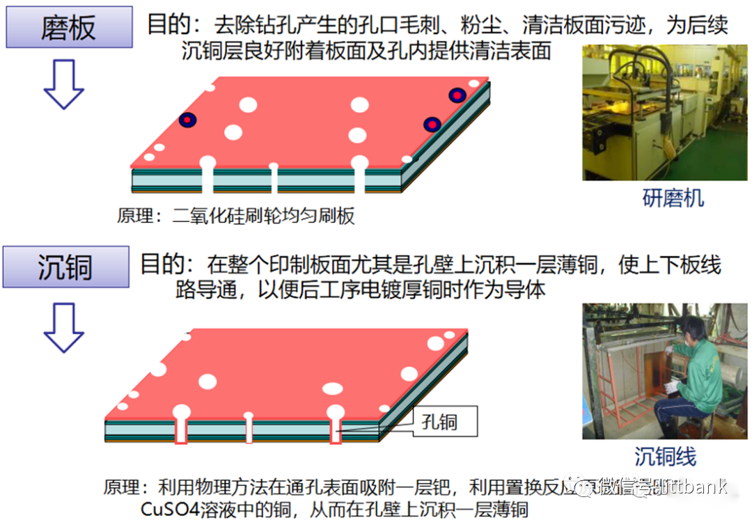
 3. PCB Raw Material Defect Cases(1) Short Circuit Defect at Xinda1. Defect description: Xinda 715G5935K01000004I D/C1316, 1317 found that the defect points were concentrated at ⑨-⑧ and the fixed circuit short circuit defect, defect rate: 21/1800=1.17%
 2. Cause analysis: It was found that in one film (1PNL with 6SET), there was 1SET with 1PCS position having a dark line.This defect occurred when the black film used for circuit production copied the yellow film, and there were black spots on the Mylar in the exposure machine that were not cleaned properly, resulting in a dark line on the copied yellow film, causing a positioning short circuit defect with the yellow film aligned with the dark line on the exposure film.
 (2) Blackening Defect on the Whole Board at San Zhao1. Defect description: On July 18, 2013, Fuzhou TPV reported a black defect in the production model 715G5074P02002002S D/C: 1325 found in SMT, defect rate: 12/300=4%
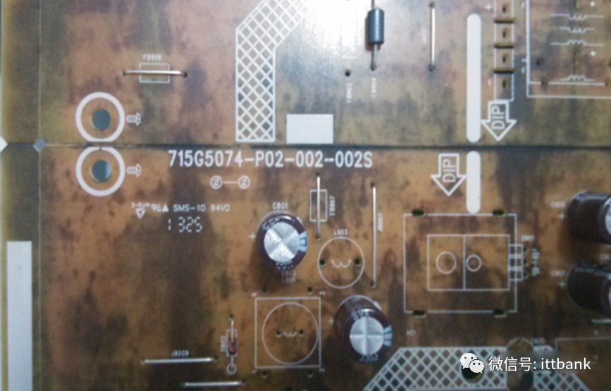 2. Cause analysis: The water washing tank in the back section of the acid washing tank has an automatic water replenishment device, but due to the operator’s negligence, this switch was not turned on during production, causing the water in the tank to not flow through the overflow outlet, leading to the blockage of the filter net at the back of the brushing wheel, causing the motor to overload, resulting in the motor automatically tripping. The control display light was previously faulty (not all lights were on during normal operation), and the water washing tank stopped working. The operator did not notice in time, causing the acid concentration in the water washing tank to increase, leaving micro-etching liquid on the board, which was carried to the conveyor roller and the sponge drying rod, causing more and more acid to accumulate on the conveyor roller and sponge rod;
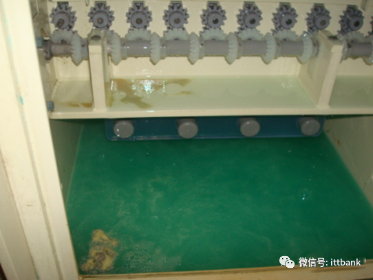 The water in the washing tank was contaminated by micro-etching solution.(3) Difficulty Inserting Due to Small Holes at Fuqiang1. Defect description: On June 6, 2013, Fuzhou TPV reported that 715G3834-M02-000-004F had small hole diameters, making it difficult to insert components, defect rate: 3.9%
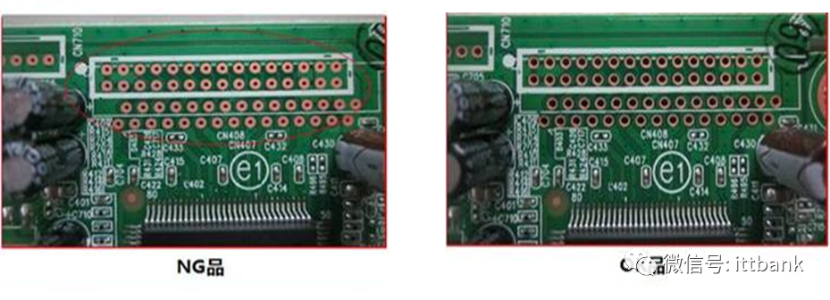 2. Cause analysis: During the drilling process for this board, a drill break occurred (the machine automatically stops and alarms during a drill break, and after handling, it continues execution). After the program is completed, supplementary drilling can be performed. The production personnel marked the board and proceeded with secondary drilling, but the drilling operator made a human error during the supplementary drilling process, using the wrong drill bit, resulting in a small diameter defect after supplementary drilling.Thus, the drilling personnel used the wrong drill bit during the secondary drilling process, and after supplementary drilling, did not distinguish the supplementary drilled board from the good board, allowing it to flow into the next process.(4) Solder Bridging Defect at San Zhao1. Defect description: On June 26, Fuzhou Guanjie complained about the San Zhao company double-sided board 715G5870M01001004S having unsoldered defects on the M line, defect rate 200/800=25%, D/C1321\1325
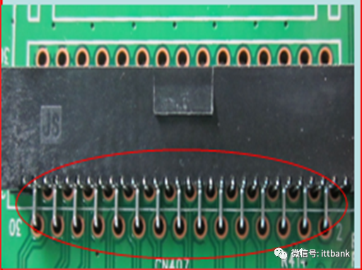 2. Cause analysis:On June 17, due to a malfunction of the air conditioning in the exposure room, the indoor temperature was relatively high, reaching 28.7°C (standard humidity: 22±5°C, usually controlled around 20-24°C). During printing, the ink at the hole mouth was relatively thin (due to the angle formed between the hole mouth and the hole wall, the ink at the corners was relatively thin and would penetrate into the hole mouth), thus after pre-baking OK, the board was placed in the exposure room for too long without controlling the placement time, and due to the high indoor temperature, the ink around the solder ring would cure, resulting in a thin layer of green oil remaining on the solder ring that was difficult to develop, causing the hole mouth to have green oil, which in turn caused the wave soldering to not adhere to the solder.
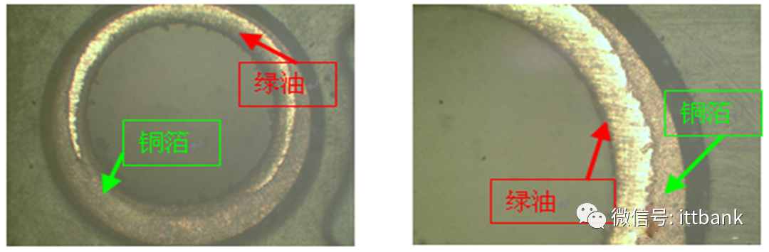 (5) Un-soldered Test Points at Jingwang1. Defect description: During mass production of 715G3834-M02-000-0H4KPCB, there were instances of test points not receiving solder (red dots), D/C: 1131
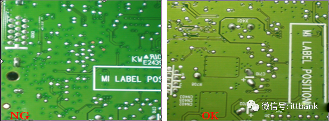 2. Cause analysis:The defect was caused by a combination of two factors: individual boards had excessively full plated holes, causing the ink on the board surface to be slightly thick, creating a certain drop from the pad of the test pad. Due to the small area of the test pad, during the soldering process, the upper limit of the OSP film thickness was difficult to decompose before immersion in solder, resulting in poor solder uptake.
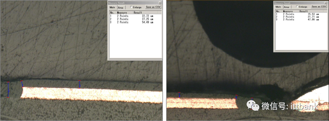 PCB Raw Material Defect Cases – Others(1) Open Circuit Defect
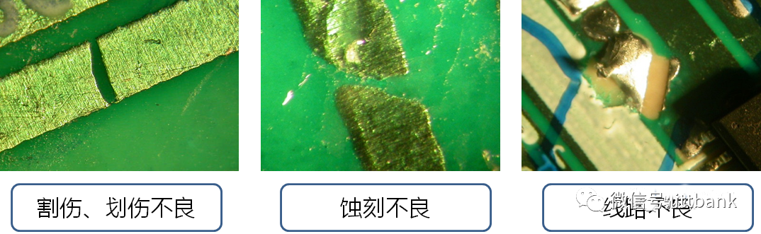 (2) Solder Pitting Defect
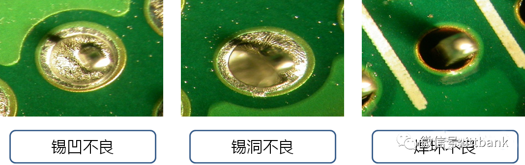 (3) Short Circuit Defect
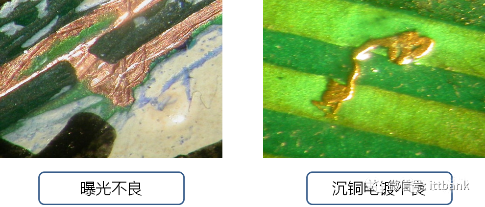 (4) Blister Defect
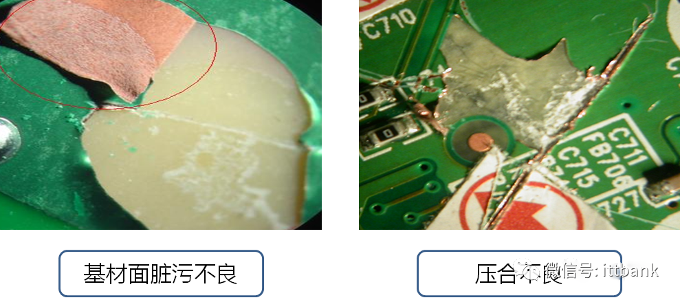 (5) Green Oil Defect
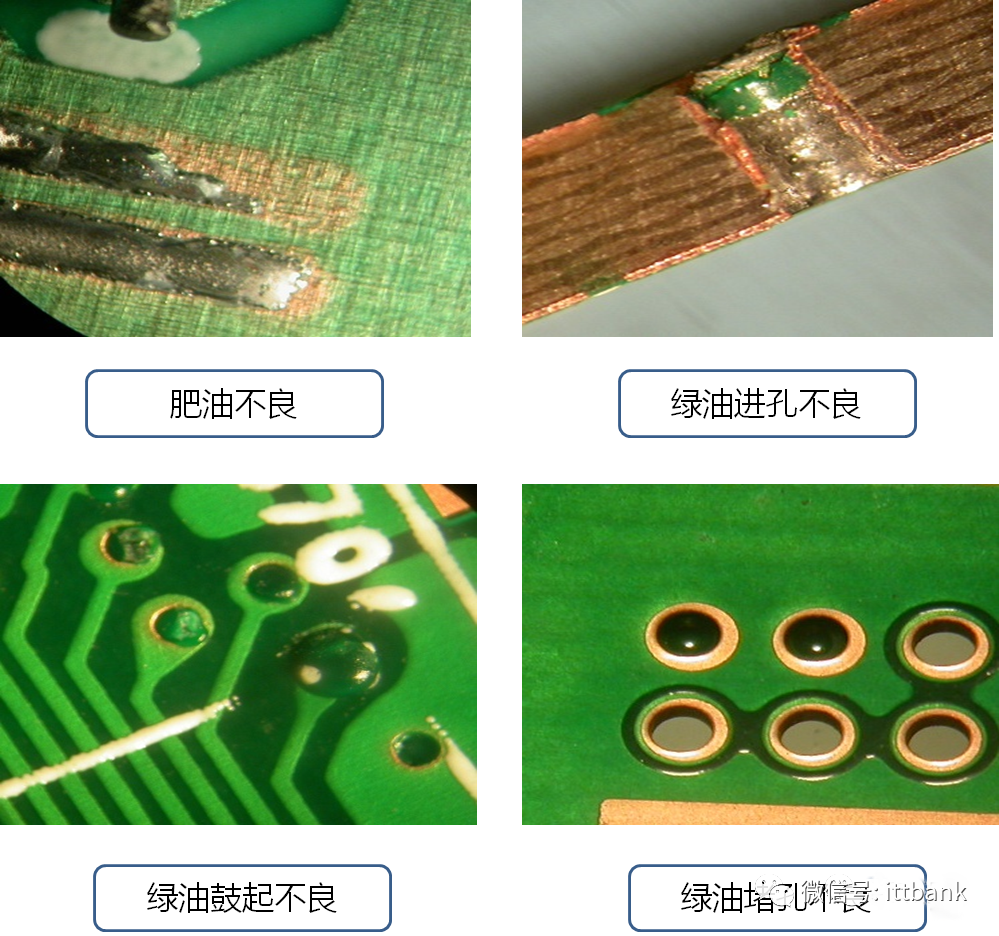 (6) Appearance Defect
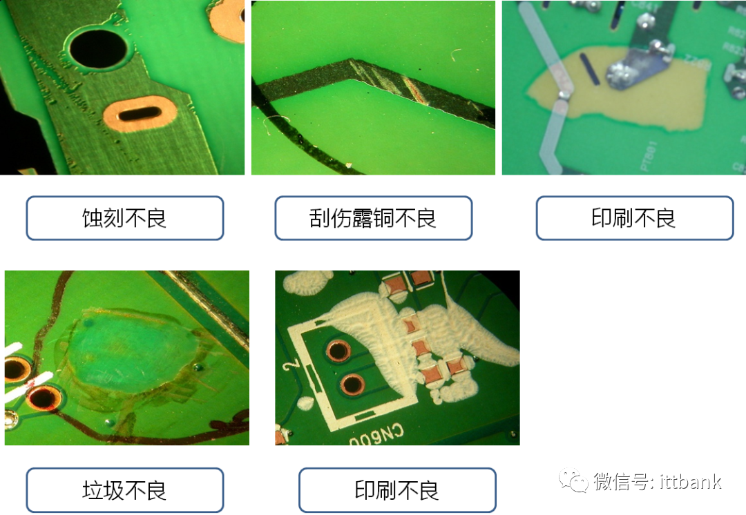 (7) V-Cut Defect
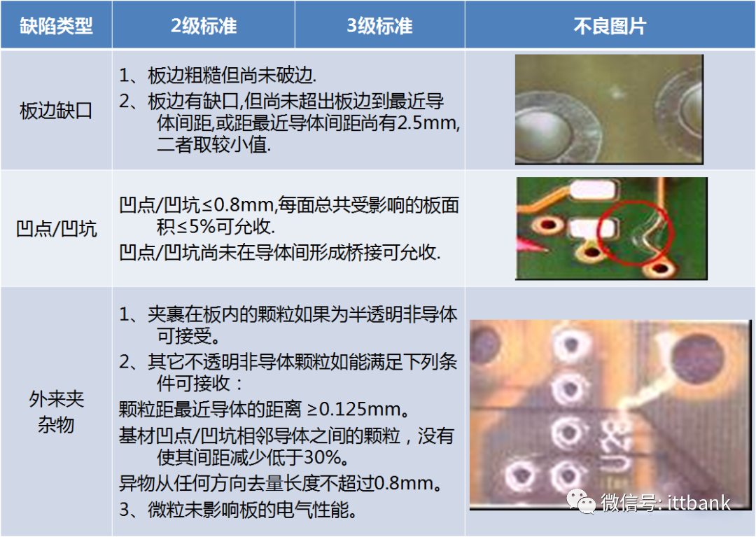
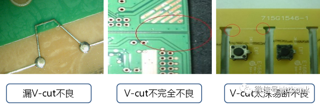 4. PCB Inspection StandardsReferences:lIPC-A-600G PCB Quality AcceptabilitylIPC-6011 Overview Performance Specification for Rigid BoardslIPC-6012 Qualification and Performance Testing Specification for Rigid BoardslIPC-TM-650 PCB Testing Methods ManuallPERFAG 3C Quality Specification for Multilayer Boards (Denmark)(1) Substrate
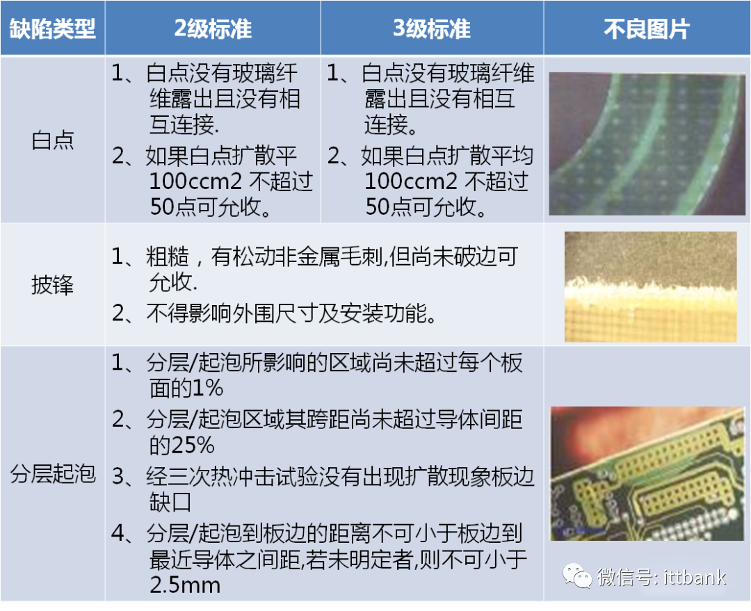
 (2) Circuit
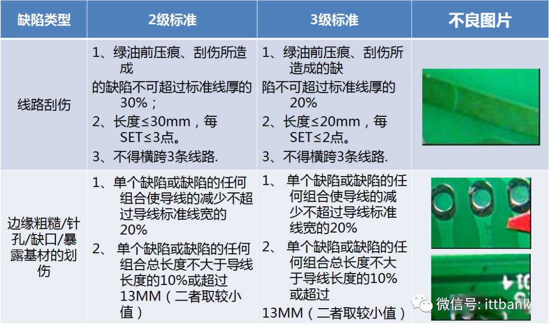 (3) Holes
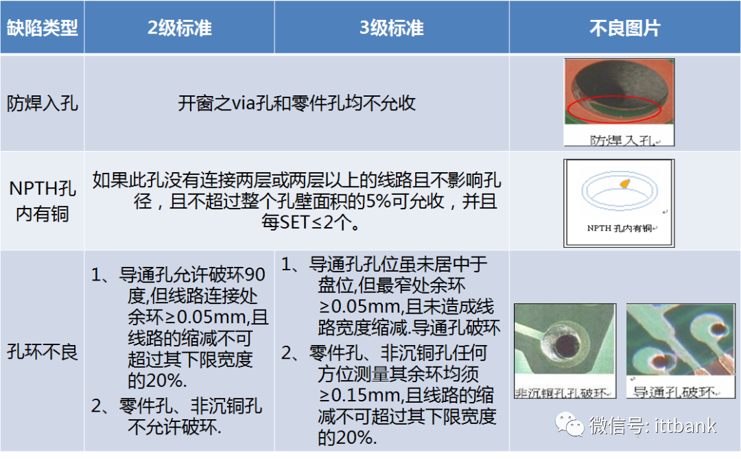 (4) Solder Mask Green Oil
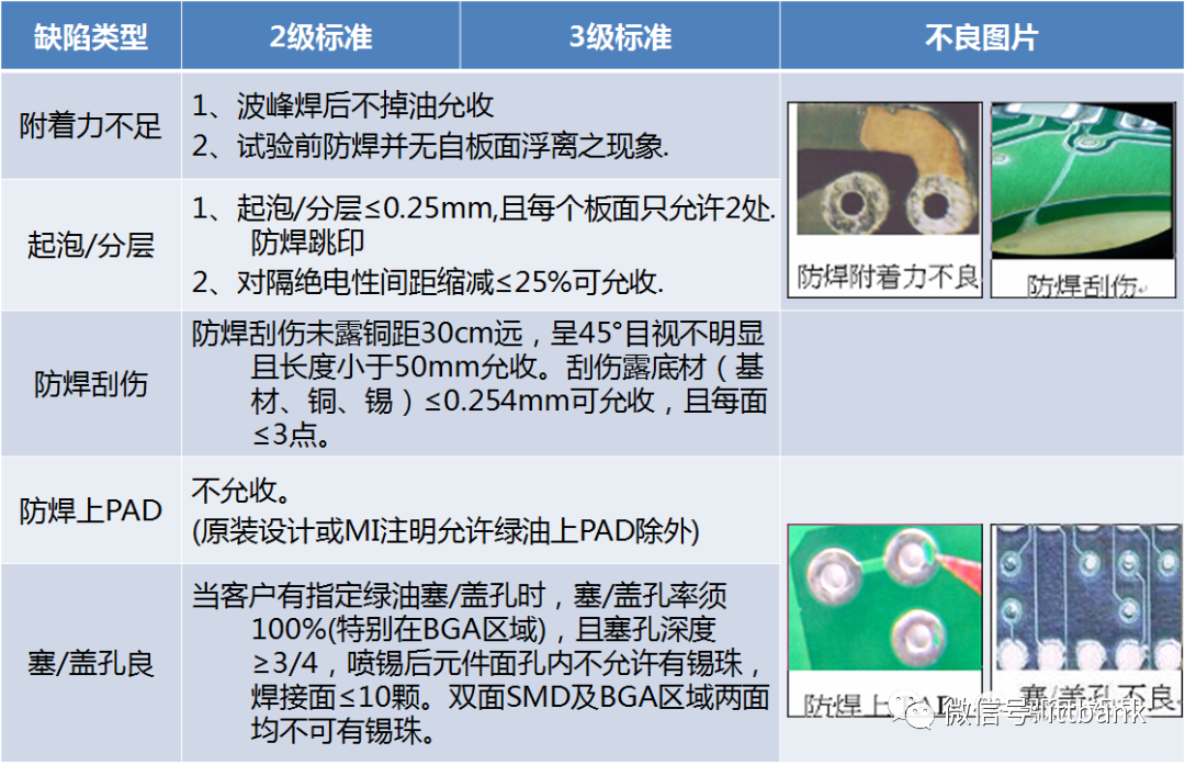 (5) Solder Coating
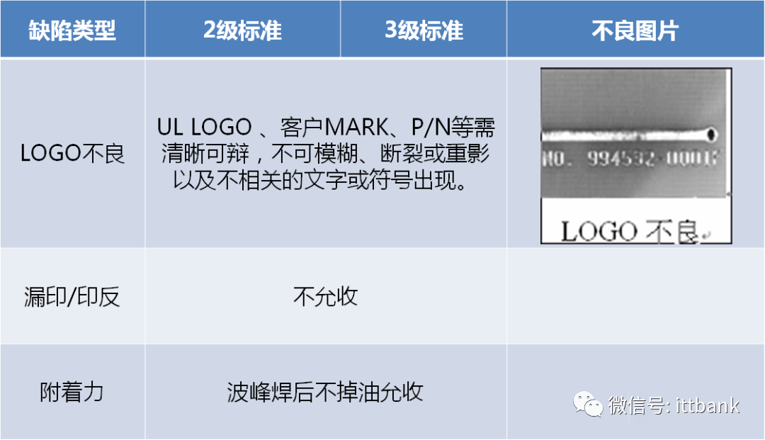
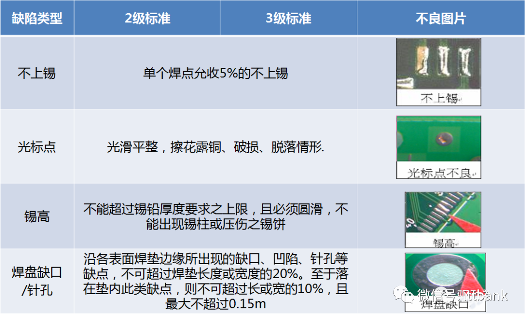 (6) Characters
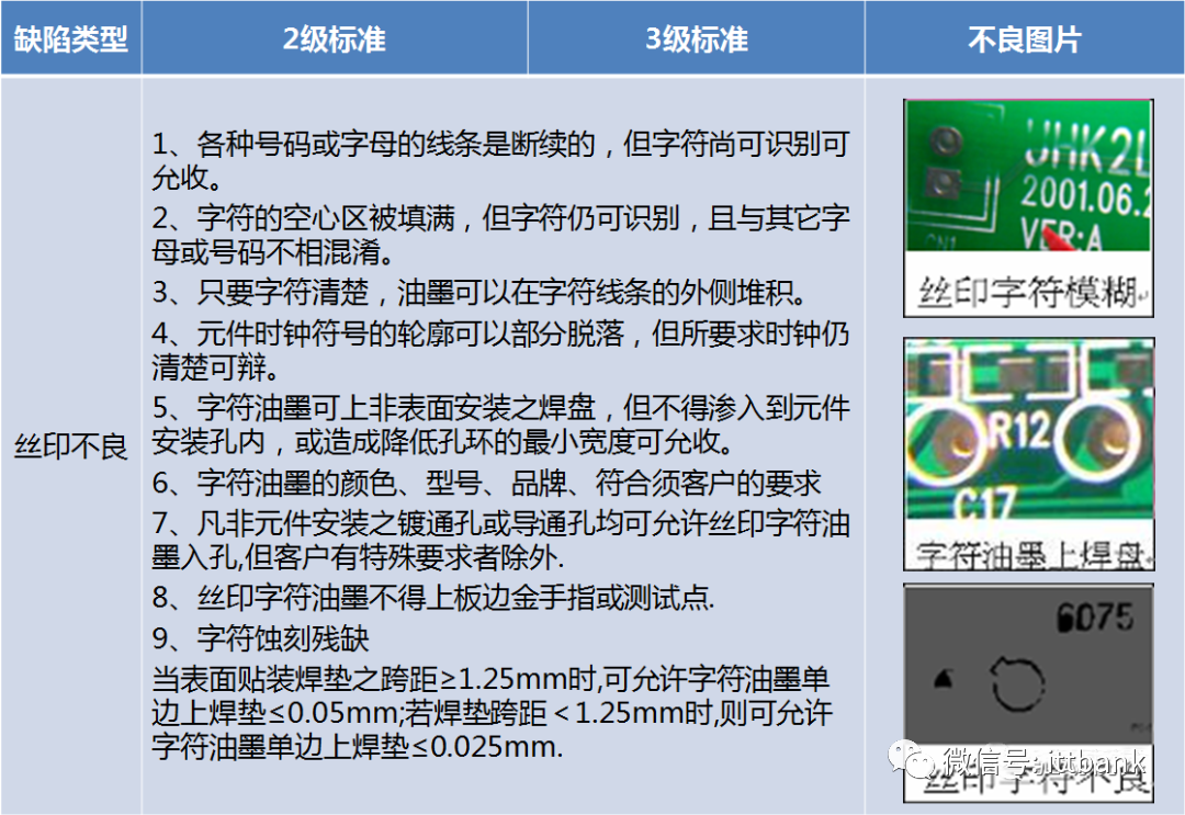
 (7) OSP
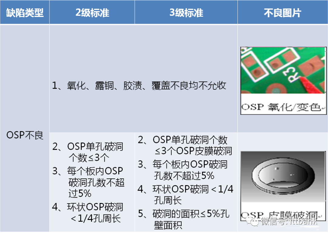 (8) Molding
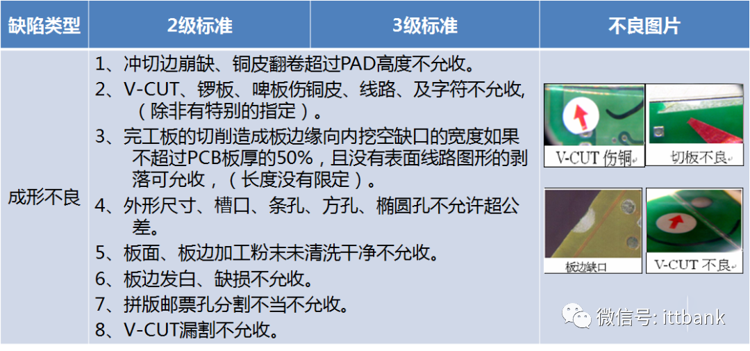 (9) Board Warping
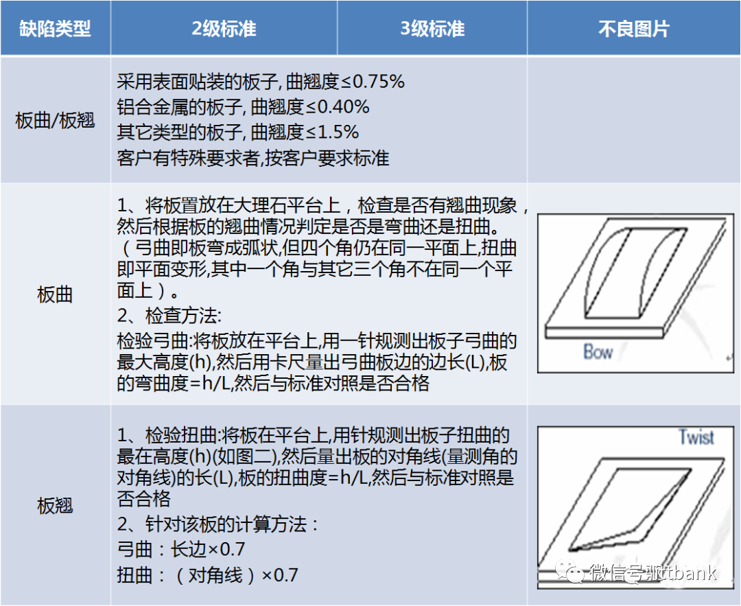
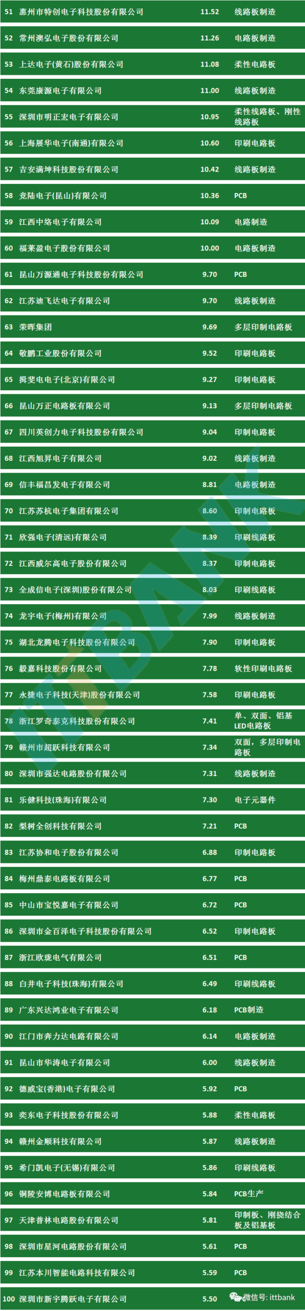
Attached PCB Manufacturers:
———— / END / ————
Note:If there are any omissions or errors, please correct them. Contact information is as follows:
Submission Email: [email protected]
ITTBANK Customer Service Hotline: 0755-5839333
Statement: Please indicate the source when reprinting!