
Talk
Chip
Weekly “Chip” News

★
★ ★ ★
★
The domestic 5nm self-developed GPU has completed tape-out verification!
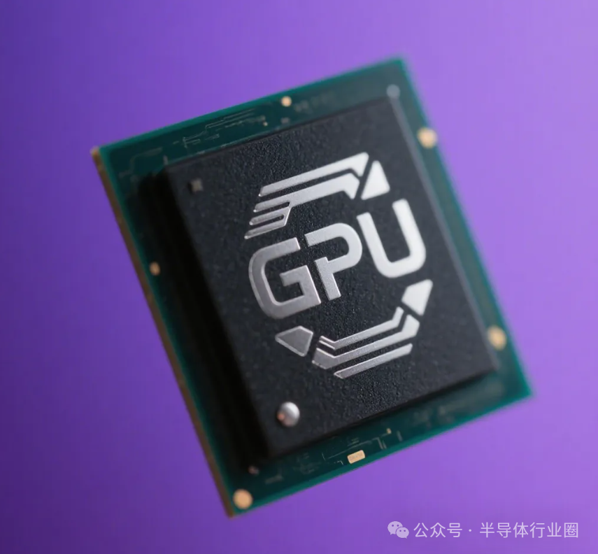
On September 4, Anfu Technology announced on its interactive platform that the new generation “Fuxi” architecture chip developed by Xiangdixian has completed tape-out verification, demonstrating excellent performance in graphics rendering and parallel computing.
It is reported that after receiving investment from Anfu Technology, Xiangdixian accelerated its product iteration. The new generation Fuxi architecture GPU will adopt a 5nm process, achieving a computing power of 160 TFLOPS (FP32) and integrating 12GB of HBM2 memory. The new generation “Fuxi” architecture chip developed by Xiangdixian is currently in tape-out, and this architecture will bring two new products, both of which meet the leading domestic performance and technical specifications. The Fuxi A0 focuses on filling the gap in domestic high-end rendering products; the Fuxi B0 is a chip that integrates GPU and NPU, targeting edge model deployment and the rapidly emerging AIPC market. The Fuxi B0 will fully support the edge deployment needs of mainstream models such as LLAMA, ChatGLM-6B, Stable-Diffusion, Sora, and DeepSeek R1 1.5B/7B.
【Source: Guoxin Network】
★
★ ★ ★
★
Congratulations! Guolian Wanzhong’s 8-inch wafer line has successfully completed wiring
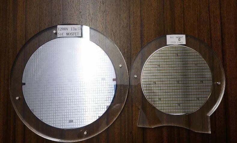
Recently, Beijing Guolian Wanzhong Semiconductor Technology Co., Ltd. (hereinafter referred to as “Guolian Wanzhong”), a leading enterprise in the third-generation semiconductor sector located in Zhongguancun Shunyi Park, announced significant news that it has successfully completed the wiring of its 8-inch silicon carbide (SiC) chip wafer process line. This milestone technological breakthrough marks a solid and critical step for our country in the third-generation semiconductor field, injecting strong development momentum into the upgrade of the domestic semiconductor industry chain.
It is reported that compared to traditional 6-inch wafers, 8-inch silicon carbide (SiC) wafers have significant advantages in production efficiency and cost control. Higher production efficiency means more chips can be produced in the same time, while lower unit costs make products more competitively priced in the market. This will undoubtedly significantly enhance Guolian Wanzhong’s position in the semiconductor market, strengthening its market competitiveness and allowing it to occupy a favorable position in the fierce market competition. Currently, the 8-inch silicon carbide (SiC) chip wafer process line has smoothly entered the product optimization and technical specification enhancement stage. After full production, the line is expected to greatly increase capacity and yield. In the fields of new energy vehicles, photovoltaic inverters, and industrial power supplies, the demand for semiconductor chips has been consistently strong. The upgrade of Guolian Wanzhong’s production line will further meet the urgent needs in these areas, providing strong chip support for the development of related industries.
【Source: Semiconductor Circle】
★
★ ★ ★
★
Chengdu Huamei Releases 4-Channel 12-Bit 40G High-Speed High-Precision RF Direct Sampling ADC Chip

On September 1, Chengdu Huamei announced that its developed 4-channel 12-bit 40G high-speed high-precision RF direct sampling ADC (Analog-to-Digital Converter) has been successfully released. The HWD12B40GA4 ADC chip developed by Chengdu Huamei is a multi-channel high-speed high-precision RF direct sampling ADC with 4 channels, a resolution of 12 bits, and a sampling rate of 40 GSPS, representing a significant breakthrough in the company’s technological innovation. This chip further enhances sampling rate, bandwidth, and other technical specifications based on the company’s existing multi-channel high-speed high-precision ADC, filling the gap in similar products both domestically and internationally, reaching an internationally leading technical level.
It is reported that this multi-channel RF direct sampling ADC chip supports configurable sampling rates of 24~40 GSPS in 4-channel mode and 48~80 GSPS in dual-channel mode. The input analog bandwidth reaches up to 19 GHz, with a noise spectral density as low as -152 dBFs/Hz, and a spurious-free dynamic range exceeding 54 dB at input frequencies within 18 GHz (Ku band). The output uses 96 pairs of JESD204C high-speed serial interfaces, supporting multi-channel synchronization functions both within and between chips, featuring high reliability. This chip adopts a fully self-developed forward design, with complete independent intellectual property rights, breaking through key technologies such as multi-channel RF direct sampling ADC architecture design, high-linearity dynamic amplifiers, and low-jitter clocks, with multiple domestic and international invention patents applied for related innovative technologies. All tape-out and packaging processes are based on domestic manufacturers, ensuring controllable production and supply.
【Source: SEMI】
★
★ ★ ★
★
Micron Semiconductor Officially Signs to Settle in Quanzhou Nanyin
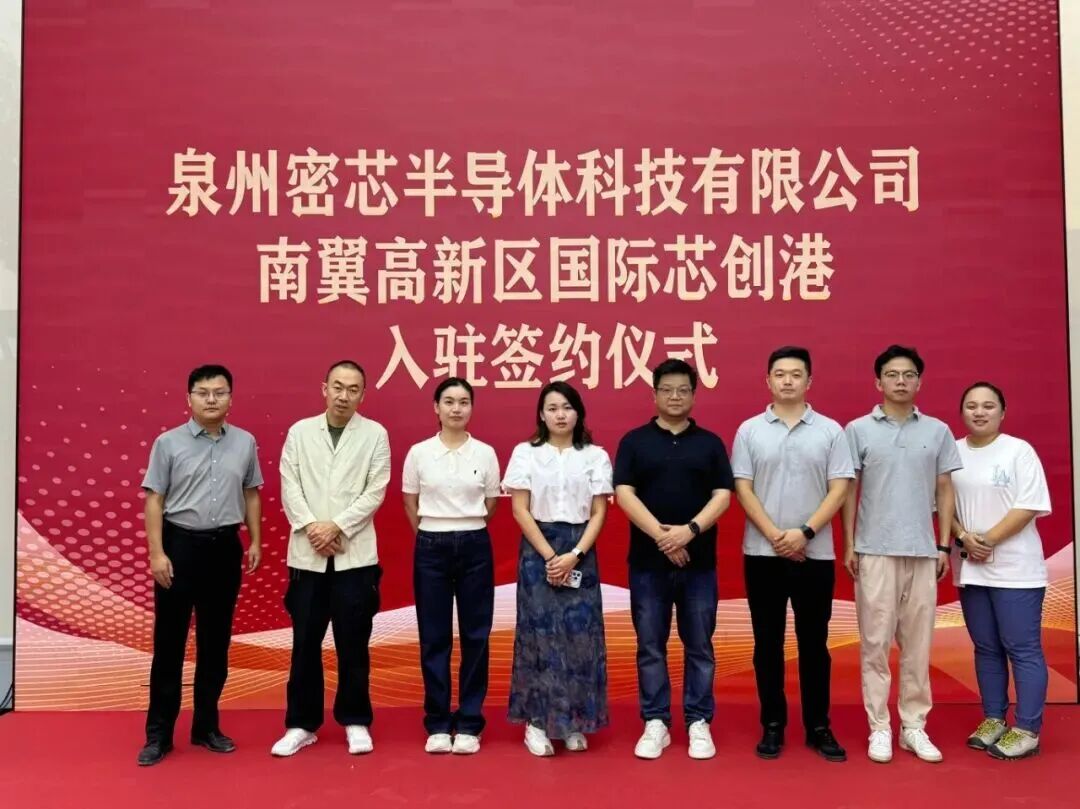
On September 3, Quanzhou Micron Semiconductor Technology Co., Ltd. officially signed an entry agreement with the Quanzhou Nanyin National High-tech Zone International Chip Innovation Port, injecting strong momentum into the high-quality development of the semiconductor industry in Quanzhou Nanyin and jointly composing a new chapter of mutual benefit and win-win.
It is understood that Quanzhou Micron Semiconductor Technology Co., Ltd. is an innovative enterprise under Yifeng Chemical, focusing on the research and development of semiconductor sealing materials and fluorinated electronic chemicals. Relying on the raw material advantages and technical accumulation of its shareholder Jiangxi Yifeng, the company continues to deepen its efforts in the semiconductor field. Its developed perfluoroether rubber (FFKM) sealing rings and other products have successfully broken the foreign monopoly, achieving import substitution and filling the gap in local high-end sealing materials for semiconductors. In the future, Micron Semiconductor will be committed to providing domestic solutions that reduce costs by more than 30% for semiconductor enterprises in Quanzhou Nanyin, greatly enhancing the resilience of the industrial chain and supply chain. In addition, the company is also actively carrying out industry-university-research cooperation, jointly developing high-temperature sealing material technology with universities, and promoting a collaborative innovation model of “Bay Area Technology + Jinjiang Manufacturing”.
【Source: Nanyin Jinjiang International Chip Innovation Port】
★
★ ★ ★
★
Huawei Announces Kirin 9020 Chip at Launch Event
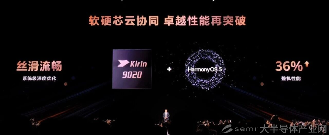
On September 4, Huawei held the “Huawei Mate XTs Extraordinary Master and All-Scenario New Product Launch Conference” in Shenzhen, officially launching its second-generation foldable flagship phone—the Huawei Mate XTs Extraordinary Master. Huawei’s Executive Director and Chairman of the Terminal BG, Yu Chengdong, announced that the Huawei Mate XTs Extraordinary Master, featuring the Kirin 9020 chip and HarmonyOS 5.0 system, marks the return of Kirin chips to Huawei’s launch event after four years. Notably, this is also the first time since 2021 that the Kirin chip has been explicitly mentioned and launched as a core selling point at a Huawei event.
In terms of performance parameters, the Kirin 9020 chip adopts a unique architecture design, with a CPU composed of 2×2.5GHz large cores, 6×2.15GHz medium cores, and 4×1.6GHz small cores, integrating the Maleoon 920 GPU, demonstrating excellent performance in multitasking and graphics rendering capabilities. The HarmonyOS 5 system provides a smoother and smarter software operating environment for the Kirin 9020 chip. The system has been optimized for foldable screen devices, with further upgrades to features such as multi-window operation and split-screen collaboration. Yu Chengdong stated that after using the Kirin 9020 chip and HarmonyOS, the phone has been deeply optimized, resulting in a 36% overall performance improvement.
【Source: SEMI】
Editor | Xu Kailin
First Review | Xu Kailin
Second Review | Yu Miao
Third Review | Chen Yang