|
1. Balance and interchange between area and speed
Here, area refers to the number of logic resources consumed by an FPGA/CPLD design. For FPGA, this can be measured by the number of used FF (flip-flops) and LUT (look-up tables). A more general measure can be the equivalent number of logic gates occupied by the design.
Speed refers to the maximum frequency at which the design can stably operate on the chip, determined by the timing conditions of the design and closely related to various timing characteristics such as clock requirements, PAD to PAD time, clock Setup Time, Clock Hold Time, and Clock-to-Output Delay.
Area and speed are the ultimate standards for evaluating the quality of FPGA/CPLD designs.
Area and speed are a pair of contradictory yet unified concepts. It is unrealistic to expect a design to have the smallest area and the highest operating frequency. A more scientific design goal should be to occupy the smallest chip area while meeting the timing requirements (including frequency requirements) of the design. Alternatively, under a specified area, the design should have greater timing margins and higher frequencies. These two goals fully reflect the idea of balancing area and speed.
As contradictory components, area and speed have different statuses. In comparison, meeting timing and operating frequency requirements is more important, and when the two conflict, a speed-first principle should be adopted.
Theoretically, if a design has a large timing margin and can operate at a speed far exceeding design requirements, then the entire design can reduce chip area consumption by reusing functional modules, thereby trading speed advantages for area savings. Conversely, if a design has high timing requirements that cannot be met by conventional methods, it can generally achieve this by converting data streams between serial and parallel formats, duplicating multiple operational modules, and employing ping-pong operations and serial-parallel conversions.
2. Hardware Principles
The hardware principles mainly refer to HDL code writing.
Verilog uses a C-like form for hardware abstraction, fundamentally serving to describe hardware! Its ultimate result is the actual circuitry inside the chip. Therefore, the ultimate standard for evaluating the quality of HDL code is the performance of the described and implemented hardware circuit, including both area and speed aspects. Evaluating a design’s code level as high only indicates that the design’s transition from hardware to HDL code representation is smoother and more reasonable. Ultimately, a design’s performance depends more on the efficiency and rationality of the hardware implementation scheme conceived by the design engineer. (HDL code is merely one form of expression for hardware design.)
Beginners who pursue neat and concise code are mistaken. This is contrary to HDL standards. The correct coding method requires a clear understanding of the hardware circuit to be implemented, a clear structure and connection of that hardware, and then expressing it using appropriate HDL statements.
Additionally, Verilog, as an HDL language, is hierarchical: system level — algorithm level — register transfer level — logic level — gate level — switch level.
Building priority trees can consume a lot of combinational logic, so wherever a case can be used, it should be preferred over IF…..else……
3. System Principles
The system principles encompass two levels of meaning: at a higher level, it refers to how a hardware system, a single board, performs module costs and task allocation, what algorithms and functions are suitable for implementation in FPGA, and what algorithms and functions are suitable for DSP, CPU, as well as FPGA scale estimation data interface design, etc. Specifically for FPGA design, there should be a macro-level reasonable arrangement for the design’s global issues, such as clock domains, module reuse, constraints, area, speed, etc. Optimization of modules at the system level is crucial.
Generally speaking, functions with high real-time requirements and fast frequencies are suitable for FPGA implementation. Compared to CPLD, FPGA is more suitable for larger scale designs with higher frequencies and more registers. When designing with FPGA/CPLD, one should have a deep understanding of the various underlying hardware resources and available design resources within the chip. For example, FPGAs generally have abundant flip-flop resources, while CPLDs have more abundant combinational logic resources. FPGA/CPLD typically consists of programmable hardware units, BRAM, routing resources, configurable IO units, clock resources, etc. The underlying programmable hardware units are generally composed of flip-flops and look-up tables. Xilinx’s underlying programmable hardware resources are called SLICE, consisting of two FFs and two LUTs. Altera’s underlying hardware resources are called LE, consisting of one FF and one LUT.
Using on-chip RAM can achieve single-port RAM, dual-port RAM, synchronous and asynchronous FIFO, ROM, CAM, and other commonly used unit modules.
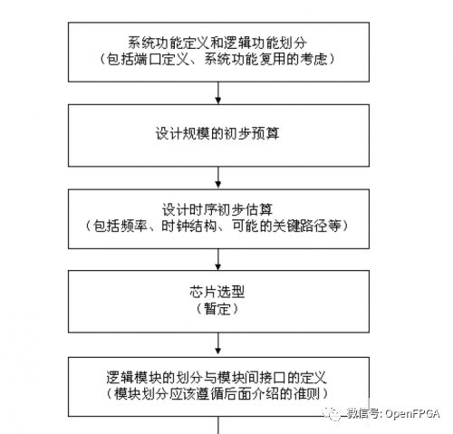
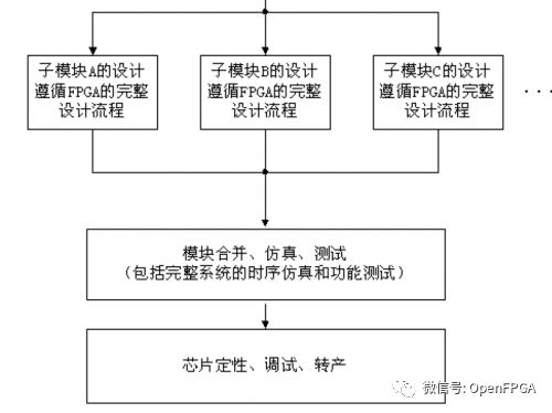
General FPGA system planning simplified process
4. Synchronous Design Principles
Asynchronous Circuits
The logical core of the circuit is implemented using combinational logic circuits. For example, asynchronous FIFO/RAM read and write signals, address decoding circuits, etc. The main signals and output signals of the circuit do not depend on any clock signal and are not driven by clock signals to produce FF outputs.
The biggest drawback of asynchronous timing circuits is the tendency to generate glitches. These glitches are particularly noticeable during simulation after layout and routing and when observed with a logic analyzer.
Synchronous Timing
The core logic of the circuit is implemented using various flip-flops.
The main signals and output signals of the circuit are generated by a clock edge driving the flip-flops.
Synchronous timing circuits can effectively avoid glitches. There are no glitches in simulations after layout and routing or in actual working signals sampled with a logic analyzer.
Does synchronous timing circuits necessarily use more resources than asynchronous circuits?
From a purely ASCI design perspective, about 7 gates are needed to implement a D flip-flop, while a gate can implement a 2-input NAND gate. Therefore, generally speaking, synchronous timing circuits occupy more area than asynchronous circuits. (This is different in FPGA/CPLD mainly due to the way unit blocks are calculated.)
How to achieve delay in synchronous timing circuits?
The common method for generating delay in asynchronous circuits is to insert a buffer or two levels of NAND gates. This method of delay adjustment is not applicable to synchronous timing design principles. First, it must be made clear that the delay control syntax in HDL is a behavioral code description, commonly used for simulation test excitation, but will be ignored during circuit synthesis and does not initiate delay effects.
Delay in synchronous timing circuits is generally achieved through timing control. In other words, the delay of synchronous timing circuits is designed as a circuit logic. For larger and special timing requirements, a high-speed clock is typically used to generate a counter, with the counter controlling the delay; for smaller delays, a D flip-flop can be used to achieve a one-clock-cycle delay, which not only delays the signal by one clock cycle but also synchronizes the signal with the clock for the first time, used in input signal sampling and increasing timing constraint margins.
How is the clock generated for synchronous timing circuits?
The quality and stability of the clock directly determine the performance of synchronous timing circuits.
Synchronization of input signals
Synchronous timing circuits require input signals to be synchronized. If the clock of the input data matches the processing clock of the chip and meets setup and hold time requirements, the main clock of the chip can directly sample the input data registers to complete synchronization. If the input data and the processing clock of the chip are asynchronous, especially when the frequencies do not match, the processing clock must sample the input data twice to achieve synchronization.
Is it guaranteed that defining as Reg type will necessarily synthesize into a register and be a synchronous timing circuit?
The answer is negative. The two most commonly used data types in Verilog, Wire and Reg, generally indicate that Wire type data is implemented through combinational logic, while Reg type data is not necessarily implemented using registers.
5. Ping-Pong Operation
Ping-pong operation is a technique commonly used in data flow control.
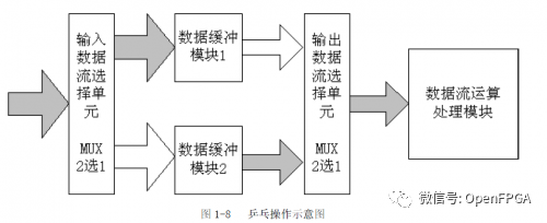
Data buffer modules can be any storage module, with common storage modules being dual-port RAM (DPRAM), single-port RAM (SPRAM), FIFO, etc. In one buffering cycle, the input data stream is cached into data buffer module 1, and in the second buffering cycle, the input data stream is cached into data buffer module 2 through the input data selection unit. The biggest feature of ping-pong operation is that through the input and output data selection units, operations and processing are conducted. Treating the ping-pong operation module as a whole, looking at data from both ends, the input and output data streams are continuous without any interruption, making it very suitable for pipelined processing of data flows. Thus, ping-pong operation is often applied in pipelined algorithms to achieve seamless buffering and processing of data.
The second advantage of ping-pong operation is that it can save buffer space. For instance, in WCDMA baseband applications, one frame consists of 15 time slots, and sometimes it is necessary to delay the entire frame of data by one time slot for processing. A direct method is to cache the frame of data and then delay it by one time slot for processing. In this case, the buffer length would be the length of one frame of data, assuming a data rate of 3.84Mb/s, one frame lasting 10ms, requiring a buffer length of 38400 bits. If ping-pong operation is used, only two buffers for one time slot of data RAM need to be defined. When writing data to one RAM, data is read from the other RAM and sent to the processing unit. At this point, the capacity of each RAM only needs to be 2560 bits, resulting in a total capacity of 5120 bits for both blocks.
Skillfully using ping-pong operation can also achieve the effect of low-speed modules processing high-speed data streams.
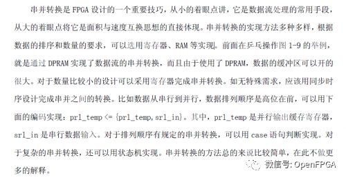
6. Serial-Parallel Conversion

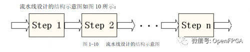
7. Pipelined Operation
Pipelined processing is a commonly used design technique in high-speed designs. If a design’s processing flow is divided into several steps and the entire data processing is unidirectional, then pipelined design methods can be considered to improve system operating frequency.
The basic structure is to chain together n operational steps that are appropriately divided and unidirectional. The greatest feature and requirement of pipelined operations is that data processing at each step must be continuous over time. If each operational step is simplified and assumed to be a clocked D flip-flop (i.e., using a register to clock a beat), then pipelined operations are similar to a group of shift registers, with data flowing through D flip-flops to complete each step of the operation. The timing diagram for pipelined design is as follows:
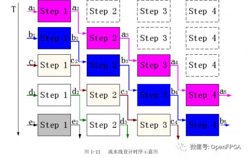
The key to pipelined design is the reasonable arrangement of the entire design timing. Each operational step must be reasonably divided. If the operation time of the previous step equals that of the next step, the design is simplest, with the output of the previous step directly feeding into the input of the next. If the operation time of the previous step exceeds that of the next, appropriate buffering is required. If the operation time of the previous step is less than that of the next, data must be split or stored and post-processed at the previous step; otherwise, overflow of downstream data will occur.
8. Synchronization Methods for Data Interfaces
Synchronization of data interfaces is a common issue in FPGA/CPLD design. Many design instabilities stem from data interface synchronization issues.
1. How to achieve data synchronization when input-output delays are unpredictable or may vary?
For unpredictable or variable data delays, a synchronization mechanism needs to be established. This can be achieved through a synchronization enable signal or a synchronization indication signal. Additionally, accessing data through RAM or FIFO can also achieve data synchronization.
Data can be stored in RAM or FIFO as follows: the data provided by the upper-level chip is written into RAM or FIFO using the accompanying clock as the write signal, and then the data is read out using the sampling clock of the current level (generally the main clock for data processing). The key to this approach is ensuring reliable writing of data into RAM or FIFO. If using synchronous RAM or FIFO, a signal with a fixed relative relationship to the data delay is required.

|


