
Click the “Read Original” at the bottom of the article to watch selected IC design courses for free!
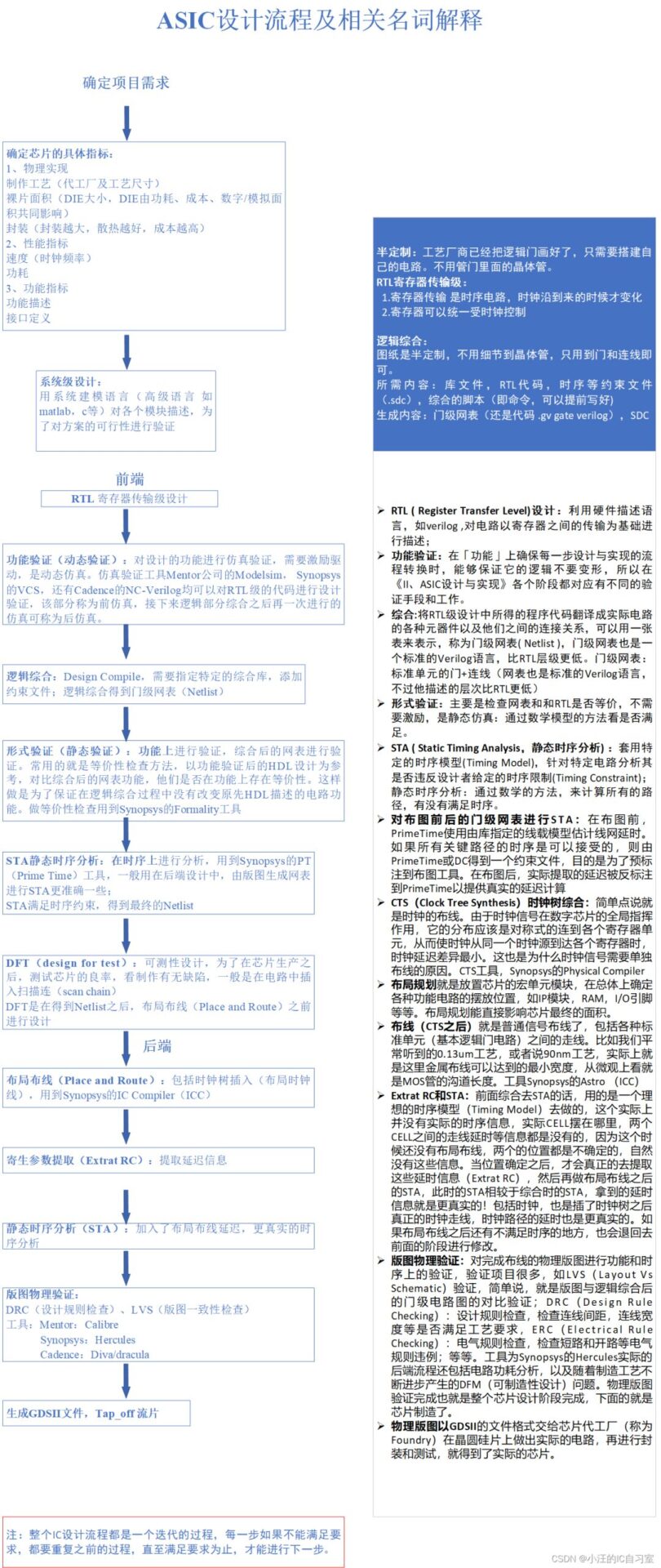
ASIC Design Process
1. Define Project Requirements
1. Determine the specific indicators of the chip:
-
Physical Implementation
Manufacturing process (foundry and process size);
Die area (DIE size, affected by power consumption, cost, digital/analog area);
Packaging (larger packaging results in better heat dissipation, but higher cost).
-
Performance Indicators:
Speed (clock frequency);
Power consumption.
-
Functional Indicators:
Function description
Interface definition
2. System-level design:
Use system modeling languages (high-level languages like Matlab, C, etc.) to describe each module to verify the feasibility of the solution.
2. Front-end Process
1. RTL Register Transfer Level Design
Use hardware description languages, such as Verilog, to describe the circuit based on the transfer between registers.
2. Functional Verification (Dynamic Verification):
Simulate and verify the functionality of the design, requiring stimulus driving; this is dynamic simulation. Verification tools include Mentor’s Modelsim, Synopsys’ VCS, and Cadence’s NC-Verilog, which can be used to verify RTL-level code. This part is called pre-simulation, and after logic synthesis, another simulation can be referred to as post-simulation.
3. Logic Synthesis (Design Compile):
Specific synthesis libraries need to be specified, and constraint files added; logic synthesis generates the gate-level netlist (Netlist).
4. Formal Verification (Static Verification):
Verify functionality using the synthesized netlist. Commonly used methods include equivalence checking, comparing the functionality of the synthesized netlist against the HDL design after functional verification, ensuring that the original circuit functionality of the HDL description has not changed during the logic synthesis process. Synopsys’ Formality tool is used for equivalence checking.
5. STA Static Timing Analysis:
Analyze timing using Synopsys’ PT (Prime Time) tool, usually used in back-end design, where layout-generated netlists provide more accurate STA;
STA meets timing constraints, resulting in the final Netlist.
6. DFT (Design for Test) Design for Testability:
To test the chip’s yield after production and check for defects, a scan chain is typically inserted into the circuit;
DFT is performed after obtaining the Netlist and before layout and routing (Place and Route).
3. Back-end Process
1. Layout and Routing (Place and Route):
Includes clock tree insertion (layout clock lines), layout and routing using Synopsys’ IC Compiler (ICC) tool.
Before routing (ordinary signal lines), layout the clock lines, which is clock tree synthesis (CTS), using Synopsys’ Physical Compiler tool.
2. Parasitic Parameter Extraction (Extract RC):
Extract delay information
3. Static Timing Analysis (STA):
Includes layout and routing delays for more realistic timing analysis
4. Layout Physical Verification:
DRC (Design Rule Check), LVS (Layout Versus Schematic)
Tools:
Mentor: Calibre
Synopsys: Hercules
Cadence: Diva/Dracula
5. Generate GDSII files, Tap-off for tape-out
(Note: The entire IC design process is iterative; if any step does not meet requirements, the previous process must be repeated until the requirements are met before proceeding to the next step.)
IC Design Process Terminology Overview (Including EDA Tools for Each Process)
Many students want to enter this industry but are not very familiar with the various positions in IC design. What should they do?
The job content, recruitment requirements, and development prospects vary for different directions. Once a direction is chosen, it can be relatively troublesome to change jobs later. So how can one determine the employment direction from the beginning?
Digital Front-end (Click to see detailed introduction)
6 months of theory + practical training, classes 3-4 days a week (20:30~22:30), with 3 teachers providing comprehensive teaching services, signing an employment agreement upon registration, and providing lifelong human resources services.
Digital Verification (Click to see detailed introduction)
6 months of theory + practical training, classes 3-4 days a week (20:30~22:30), with 3 teachers providing comprehensive teaching services, signing an employment agreement upon registration, and providing lifelong human resources services.
Digital DFT (Click to see detailed introduction)
6 months of theory + practical training, classes 3-4 days a week (20:30~22:30), with 3 teachers providing comprehensive teaching services, signing an employment agreement upon registration, and providing lifelong human resources services.
Digital Back-end (Click to see detailed introduction)
6 months of theory + practical training, classes 3-4 days a week (20:30~22:30), with 3 teachers providing comprehensive teaching services, signing an employment agreement upon registration, and providing lifelong human resources services.
Analog Design (Click to see detailed introduction)
6 months of theory + practical training, classes 3-4 days a week (20:30~22:30), with 3 teachers providing comprehensive teaching services, signing an employment agreement upon registration, and providing lifelong human resources services.
Analog Layout (Click to see detailed introduction)
4 months of theory + practical training, classes 3-4 days a week (20:30~22:30), with 3 teachers providing comprehensive teaching services, signing an employment agreement upon registration, and providing lifelong human resources services.
Having a general understanding of the job content, what preparations should one make to enter the target position? Datong University has selected 6 major IC design job employment courses for free trial! Gain a deeper understanding of IC design to help clarify your career choices!
Scan to add WeChat of Frog Brother 👇
Reply “IC Design” to view the course outline
Get selected trial classes from senior engineers
Receive a channel-exclusive 2000 RMB discount coupon

Teaching Object
Master’s degree or above
or students majoring in electronics or related fields
Learning Outcomes
Comprehensive professional skills required for digital IC design positions
Enterprise-level tape-out project experience
Course Schedule
20:30~22:30
(3-4 days a week)
Practical Training (2 months)

1. Project Kickoff Meeting

2. Project Breakdown
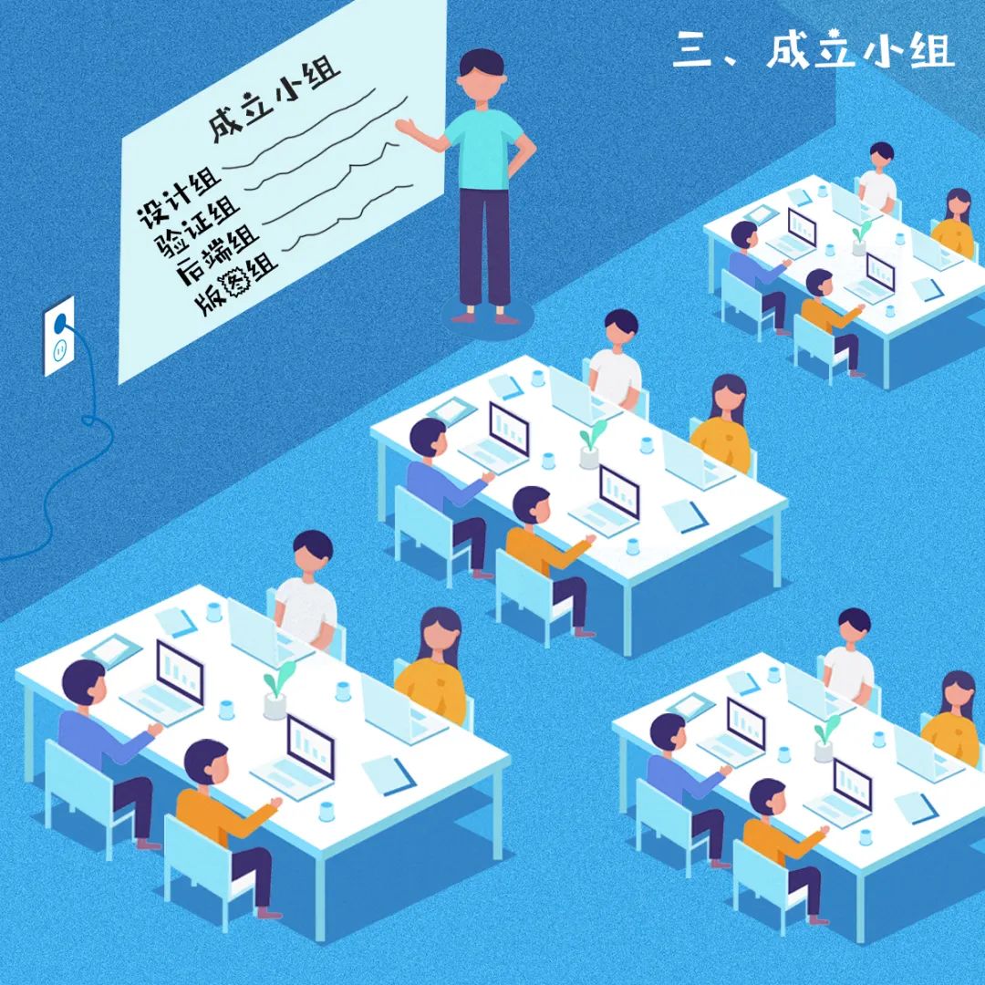
3. Establishing Various Groups

4. Daily Standup Meetings

5. Weekly Project Meetings

6. Key Challenge Groups

7. Review of Each Stage
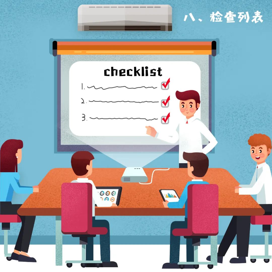
8. Checklist
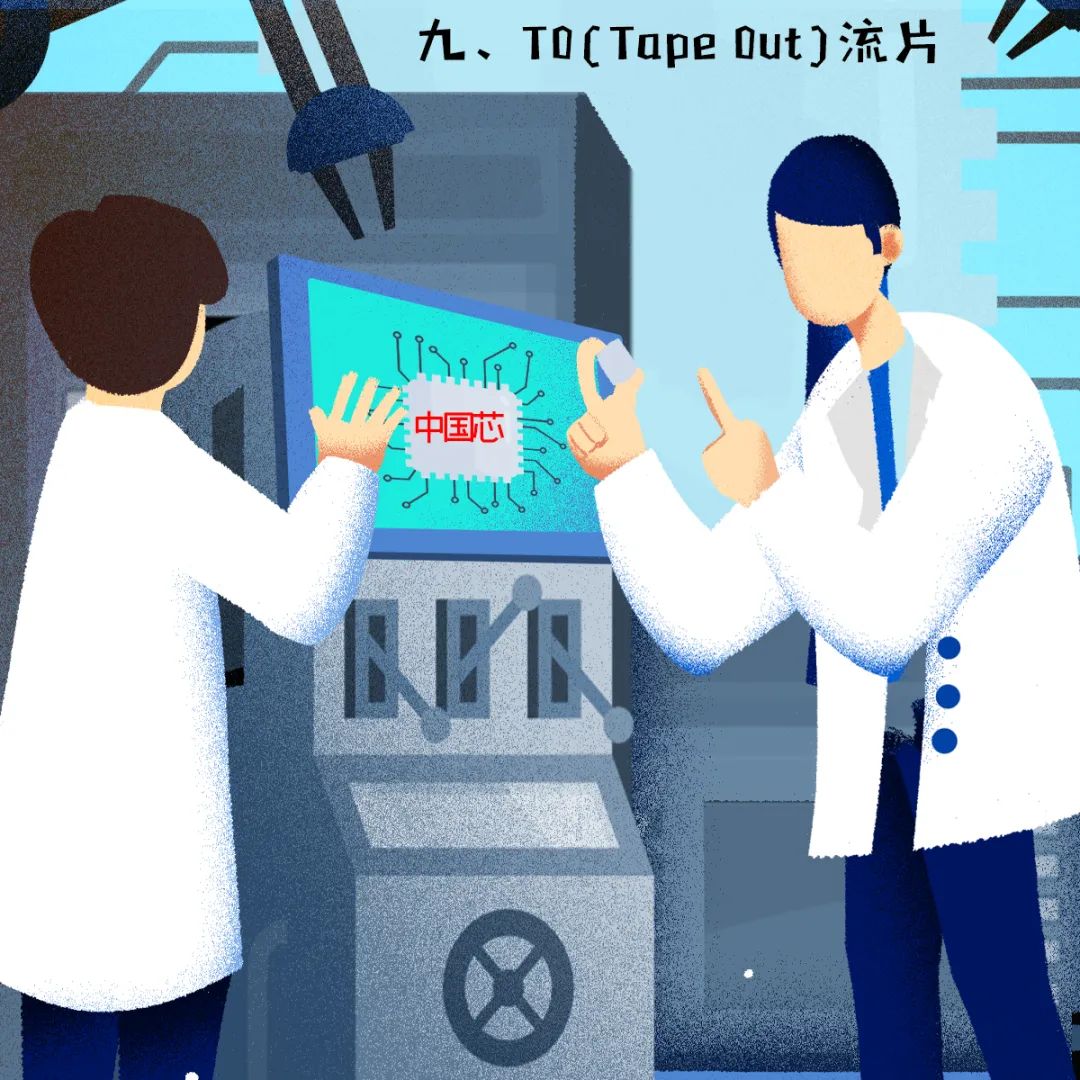
9. Tape-out
Teacher Assignment
Instructor: 15+ years of experience in major companies, scheduled classes
Teaching Assistant: Available for questions at any time
Teaching Management Teacher: Supervises learning status
Employment Guidance
Resume polishing
15+ technical experts for mock interviews
Employment recommendations from partner companies
Career planning guidance
Provides lifelong human resources services
Employment agreement signed upon registration
If not employed within 3 months after graduation
Full refund!
Full refund!
Full refund!
Need to know more
Scan to add WeChat of Frog Brother 👇
Reply “IC Design” to view the course outline
Get selected trial classes from senior engineers
Receive a channel-exclusive 2000 RMB discount coupon

Recommended Reading:
1.Transitioned from testing position to digital front-end, landed a 390K high salary offer
2.Started learning digital back-end in the second year of graduate school, signed a 400K high salary offer in autumn recruitment
3.Jumped out of “dead-end majors” early, became an “offer collector”
4.From IC novice to receiving a 450K offer during autumn recruitment
5.Made time to learn IC, finally signed a 320K high salary offer
6.After 6 months of learning IC verification, students are torn between which offer to choose


Some materials are sourced from CSDN blogger “Xiao Wang’s IC Study Room”
If there is any infringement, please contact for authorization or deletion