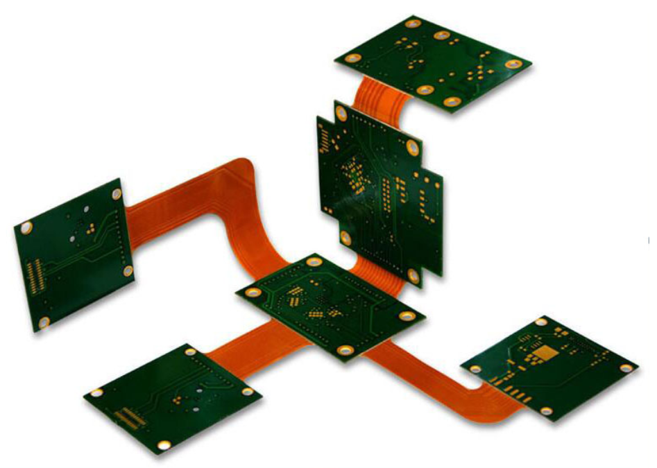
In this article, we focus on the Rigid-Flex Multi-zone design and materials.
1. Multi-Zone
Multi-zone refers to dividing a complete substrate into multiple parts, each of which may have different thicknesses and stack-ups.
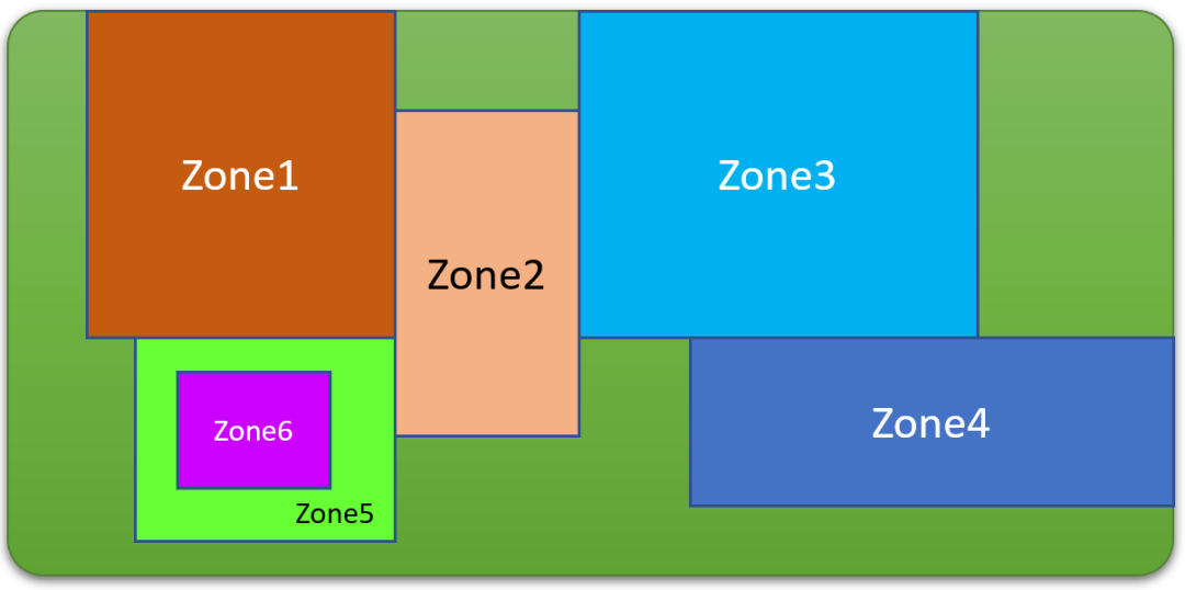
Moreover, we need to understand that not all areas of a Rigid-Flex circuit need to define zones. For areas without defined zones, the stack-up defaults to the Primary stack-up. For example, in the image below, the stack-up structure for the area without a defined zone is the Primary stack-up.
From the image below, we can see that zones can be independently defined on the substrate, they can be adjacent or non-adjacent, but cannot overlap. Additionally, zones can be nested, meaning one zone can be completely within another zone, such as zone 6 being nested within zone 5, referred to as Nested-zone. The stack-up of nested zones is also completely independent, with no dependency.
-
Multi-stackup and Multi-zone
From a physical structure perspective, Multi-stackup is defined on the Z-axis of the substrate, while Multi-zone is defined on the XY plane of the substrate. They are relatively independent but interdependent; they are combined through mapping.
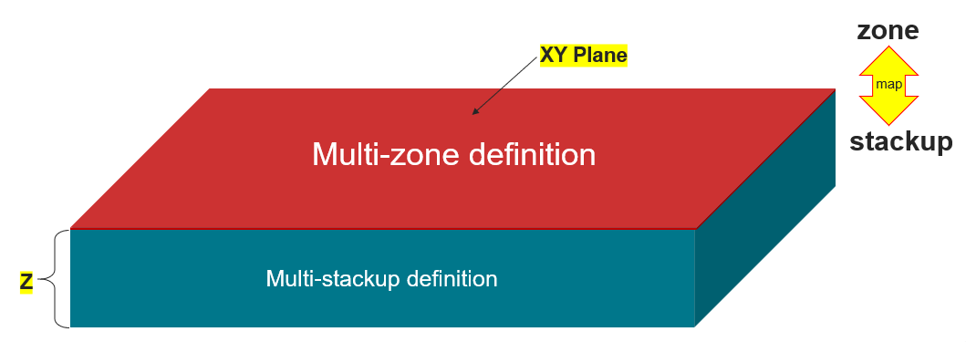
Generally, we first define Multi-stackup, then define Multi-zone, and then map zones and stack-ups to each other.
Multi-stackup and Multi-zone are interdependent; although they can exist independently in design tools, without one, the other will lose its original function.
First, define Multi-stackup:

Then define Multi-Zone and map different zones to the corresponding stack-up. Different zones can use the same stack-up. To avoid confusion, if the stack-up is named A, the zones using that stack-up A are usually named zone A1, zone A2, zone A3… and so forth.
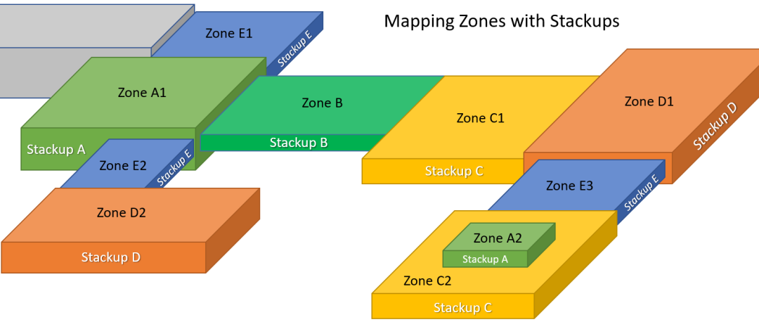
The definition of Multi-Zone in design and its mapping with Multi-stackup.
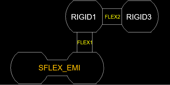
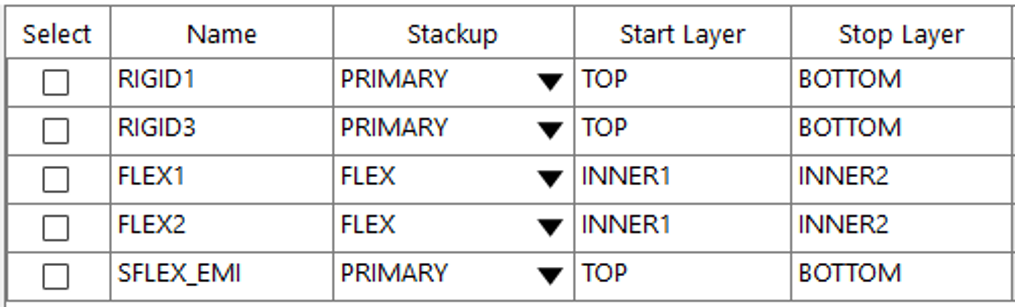
In chip manufacturing, almost all elements of the periodic table are exhaustively utilized, and the materials applied in packaging and board-level systems are increasingly diverse.
Due to its Multi-bending, Multi-stackup, and Multi-zone characteristics, Rigid-Flex utilizes a much wider range of materials compared to traditional substrates. We categorize material applications into three major types: dielectric materials, conductor materials, and mask materials.
-
Dielectric Material
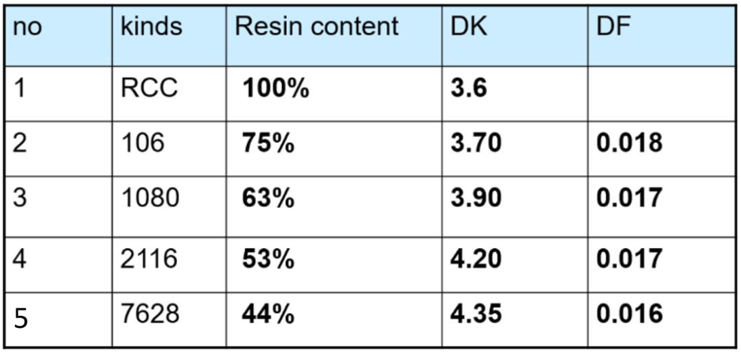
The image below shows the materials of a 2+4+2 stacking structure substrate; we can see that 106, 2116, and 7628 are all used.
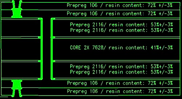
Of course, such a thick substrate can only be applied in the rigid areas of Rigid-Flex; for flexible areas, due to bending requirements, the layer count is lower, and its dielectric material will use more flexible polyimide.
-
Conductor Material
Conductor materials on Rigid-Flex substrates are usually copper foil. The commonly used copper foil thickness for rigid substrates is 17μm (half an ounce), 35μm (one ounce), 70μm (two ounces), and so on.
Copper foil thickness is directly proportional to current capacity; if a larger current is needed, thicker copper foil and wider wiring should be selected.
The table below shows the relationship between line width, copper thickness, temperature rise, and current capacity for reference.
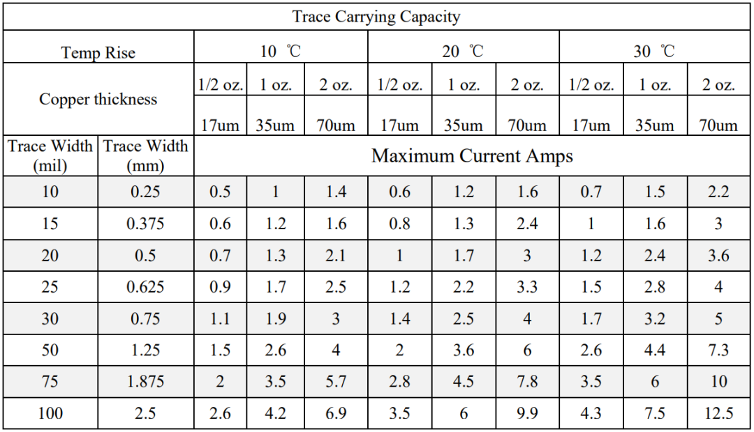
Flexible substrate copper foil is comparatively thinner, with specifications of 5μm, 9μm, 12μm, 16μm, 22μm, etc. being more commonly used on flexible boards.
-
Mask Material
There are various types of mask layers in Rigid-Flex, typically including: Soldermask, Coverlay, EMI Shielding, Selective Plating, Stiffener, etc.
These mask layers can be divided into two main categories: conductor masks and non-conductor masks.
The material for Soldermask is usually epoxy-based, initially in liquid form, and solidifies to adhere to the substrate surface. New types include LPI or LPISM (Liquid Photo Imageable Soldermask), which is a two-component liquid ink that is mixed before application to maintain its shelf life. LPI is superior to epoxy-based liquid in terms of precise printing, better contact with PCB, and increased durability.
Selective Plating involves metallizing the pads or specific surfaces of the substrate, with materials including copper, gold, silver, and other good conductors.
The materials for Stiffeners are divided into insulating materials and conductor materials; since there is no electrical connection with the substrate, structural strength is the main consideration. Insulating materials can include FR4, POLYMIDE, etc., while conductor materials typically use stainless steel.
3. Conclusion
Multi-bending, Multi-stackup, and Multi-zone are the three fundamental characteristics of Rigid-Flex circuits. Coupled with the application of dielectric materials, conductor materials, and mask materials, readers can essentially master the design and application of Rigid-Flex circuits.
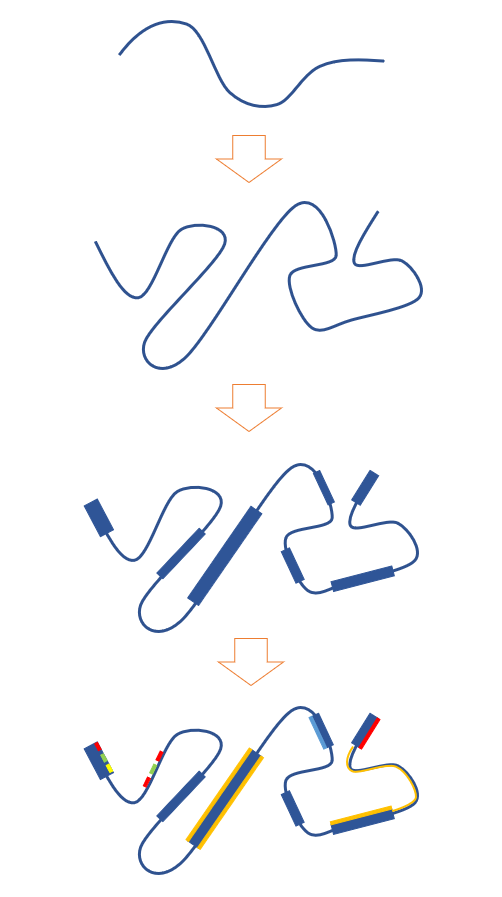
Rigid-Flex circuits are often more complex than we imagine. When I first encountered Rigid-Flex, I thought it was just a circuit with more bending functionality than ordinary circuits, only to later realize how shallow my understanding was.
The image below roughly illustrates the change in my understanding of Rigid-Flex circuits. Our understanding of the world generally undergoes a similar process.
END
1. Implementation and Application of Nano-Electron Beam Lithography Systems
2. Can Quantum Chips Bear the Burden of Computing Power?
3. Electromagnetism, Magnetoelectronics, and Magnetoelectronics
5. Research on Organic-Inorganic Hybrid Copper(I) Halide Scintillators
6. Constructing LVTSCR ESD Circuit Simulation Models Using BJT Mextram Models