Click 👇 to follow, set the “…” key in the upper right menu as a star to avoid missing the latest tweetsIt is believed that almost all electronic practitioners will encounter the I2C communication protocol. I2C (Inter-Integrated Circuit) bus is a two-wire synchronous serial communication protocol developed by Philips Semiconductors (now NXP) in the 1980s, mainly used to connect microcontrollers with peripheral devices (such as sensors, memory, etc.). Its core value lies in achieving multi-device communication with minimal wiring, greatly simplifying hardware design.This article will provide a detailed explanation of I2C from various aspects including physical structure, electrical characteristics, and core communication protocols.
01
—
Basic Overview
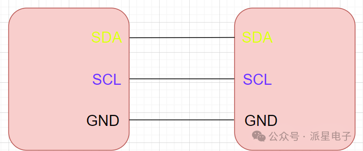
The IC bus supports any IC manufacturing process (NMOS, CMOS, bipolar). The two lines – Serial Data Line (SDA) and Serial Clock Line (SCL) | transmit information between devices connected to the bus.
Each device has a unique address for identification (whether it is a microcontroller, LCD driver, memory, or keyboard interface), and can act as either a transmitter or receiver (depending on the function of the device).
The master device initializes the bus for data transmission and generates the clock signal that allows transmission. At this time, any addressed device is considered a slave.
02
—
Main Features
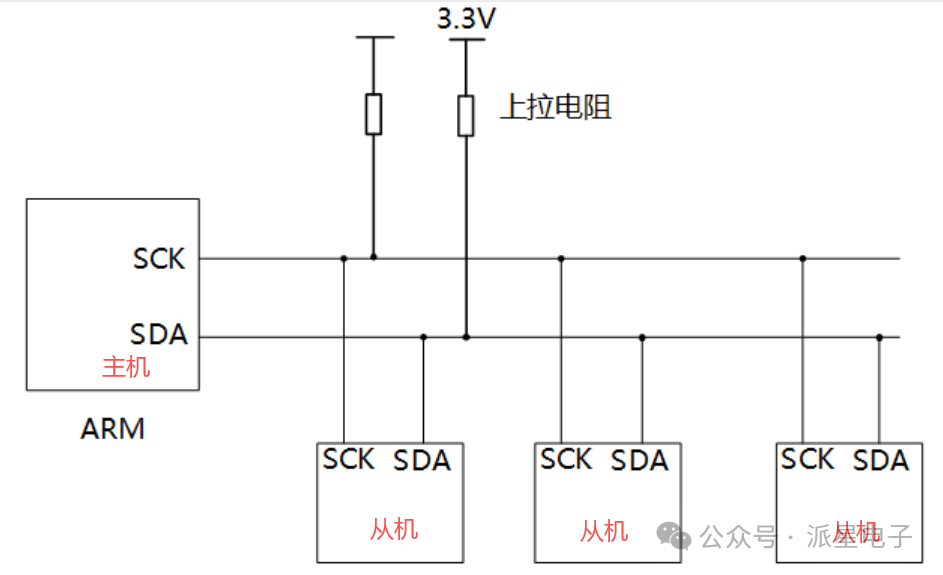
SDA and SCL are both bidirectional lines, connected to the positive power supply voltage through a current source or pull-up resistor. When the bus is idle, both lines are at a high level.
The output stage of devices connected to the bus must be open-drain or open-collector to perform the wired-AND function,
SCL and SDA both require pull-up resistors (generally determined by the power supply voltage and bus capacitance) to ensure data stability and reduce interference.
The data transmission rate on the I2C bus can reach 100 kbit/s in standard mode, 400 kbit/s in fast mode, and 3.4 Mbit/s in high-speed mode.
The number of interfaces connected to the bus is limited only by the maximum bus capacitance of 400 pF.
The bus has very low current consumption, strong anti-noise interference capability, and increasing the bus driver can expand the bus capacitance by ten times, allowing transmission distances of up to 15 m.
Compatible with devices of different voltage levels, the bus sets the reference level through simple pull-up resistors, for example, when the pull-up resistor is connected to a 5V power supply, the bus logic high level is 5V; if connected to a 3.3V power supply, the high level is 3.3V.
03
—
IIC Bus Mounting Method
The I2C bus can be online detected through external wiring, facilitating system fault diagnosis and debugging, allowing faults to be immediately addressed. Software also benefits from standardization and modularization, shortening development time.
On the <span>I2C</span> bus, each slave has its unique device address. Therefore, we only need to know the device’s address, and based on the timing, communication between the microcontroller and the device can be achieved.Note that based on practical design experience, it is generally no more than 8 devices.
The theoretical number of slaves on the I2C bus is determined by the address space: a 7-bit address provides 128 combinations, and after deducting the broadcast bit and reserved address 0x00, theoretically, IIC can mount up to 127 devices. However, the protocol does not directly limit the number of devices but stipulates that the bus capacitance must not exceed 400 pF. Due to the presence of device pin input capacitance and PCB parasitic capacitance, it is usually recommended in practical design to mount no more than 8 devices to ensure signal integrity.
The IIC bus adopts an open-drain (OD) output structure, which determines that it must rely on external pull-up resistors to establish a high level. However, the pull-up resistor and the parasitic capacitance on the bus together form an RC circuit, and its time constant will directly cause the signal edges to become smooth, leading to signal integrity issues. As the communication rate increases, the time window for each bit will shorten accordingly, requiring the signal’s rise/fall edges to be steeper. Therefore, to maintain reliable timing under high-speed transmission, the RC time constant must be strictly controlled, which requires selecting appropriate pull-up resistors or optimizing layout to reduce bus capacitance.
04
—
Working Timing
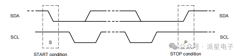
1. Start/Stop Conditions: The only occurrences in the I2C bus are defined as start S and stop P conditions.
Start Signal (START/S): SCL remains high, SDA transitions from high to low, waits for a short period, and then SCL goes low.
Stop Signal (STOP/P): SCL remains high. SDA transitions from low to high.
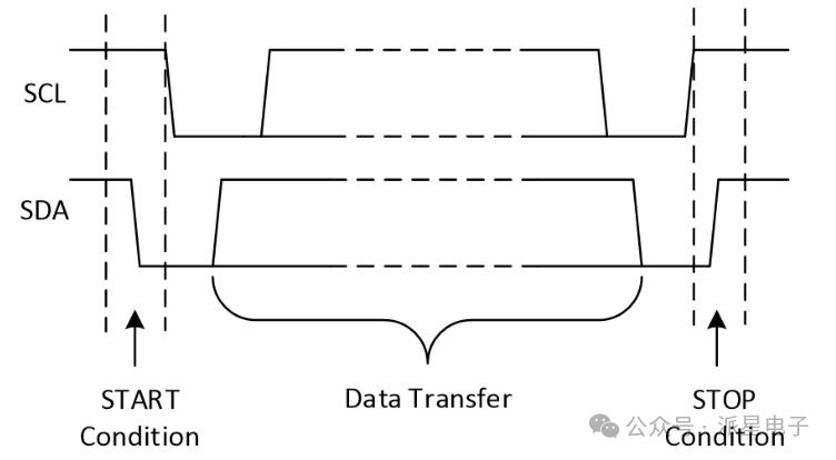
2. Idle State: After the start condition is generated, the bus is in a busy state, exclusively occupied by the master and slave devices of this data transmission, while other I2C devices cannot access the bus; after the stop condition is generated, the master and slave devices of this data transmission will release the bus, and the bus will be idle again.
3. Acknowledge Signal: During the acknowledge clock pulse (SCL is high), the master will read the level state of the SDA line. If the slave pulls SDA low, it generates a valid acknowledge signal (ACK), indicating that it has successfully received the data; if SDA is high, it is a non-acknowledge signal (NACK), usually indicating a reception failure.
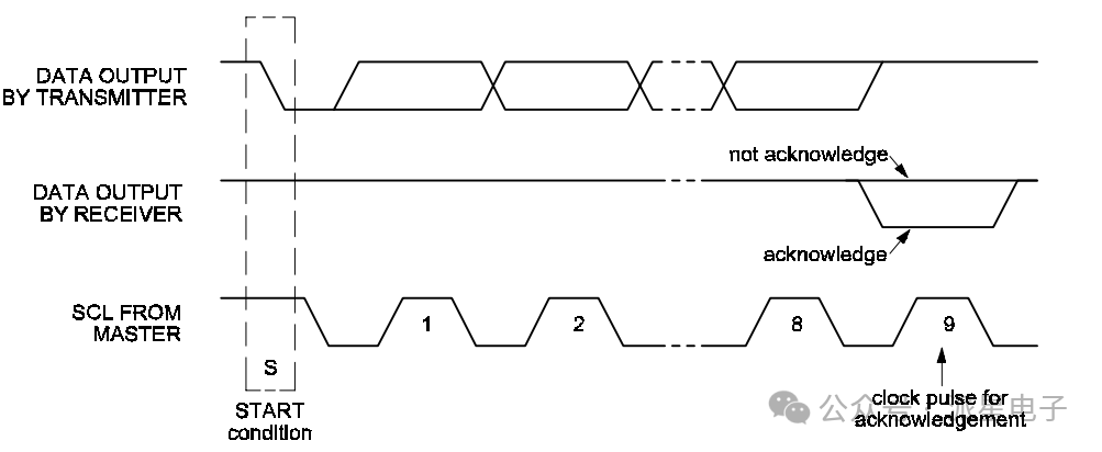
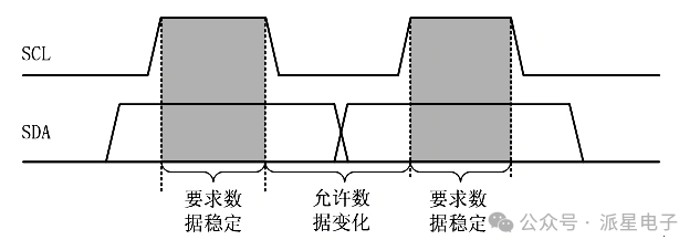
4. Data Validity: During I²C bus data transmission, the level state of the data line SDA is only allowed to change during the low level of the clock line SCL. Once SCL goes high, SDA must remain absolutely stable, with no transitions. Any changes in SDA level during SCL high will be interpreted by the bus as the start (S) or stop (P) signal of the control transmission, rather than a data signal.
05
—
IIC Timing Diagram
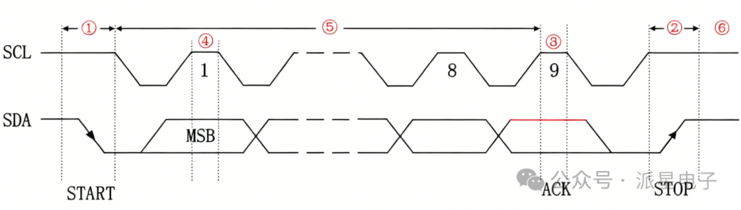
Through the IIC timing diagram, the following six key steps clearly show a complete I2C data read/write timing.
The corresponding steps of the following numeric icons:
-
Start Signal
-
Stop Signal
-
Acknowledge Signal
-
Data Validity
-
Data Transmission
-
Idle State
06
—
IIC Master Write Timing Example
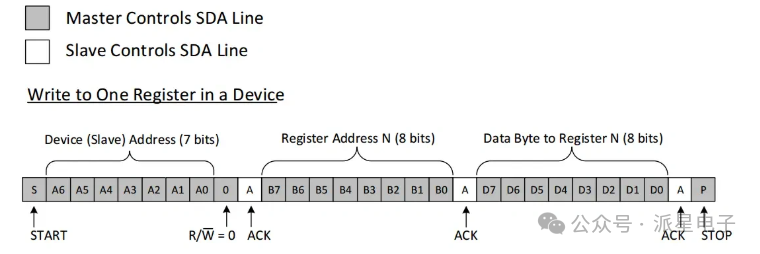
IIC write timing: To write on the I2C bus, the master will send on the bus: a start flag, the slave address, and the last bit (R/W bit) set to 0, indicating a write operation. After the slave sends an ACK response confirmation, the master will send the register address of the register it wishes to write to. The slave will confirm again, letting the master know it is ready. After this, the master will start sending register data to the slave until the master has sent all the data it needs (sometimes just one byte), and the master will terminate the transmission with a stop condition.
The specific steps are as follows:
1. Start Signal.
2. Send I2C device address, each I2C device has a device address, and the specific device address is sent to determine which I2C device to access. This is an 8-bit data, where the high 7 bits are the device address, and the last bit is the read/write bit (1 indicates a read operation, 0 indicates a write operation). 3. Read/write control bit, since data is being sent to the I2C slave device, it is a write signal 0.
4. ACK response signal sent by the slave.
5. Resend Start Signal.
6. Send the register address to write data.
7. ACK response signal sent by the slave.
8. Send the data to be written to the register.
9. ACK response signal sent by the slave.
10. Stop Signal.
07
—
IIC Master Read Timing Example
To read data from the slave device, the master must first indicate which register it wishes to read data from. This is done by starting the transmission in a similar way to writing to the slave device, by sending the address with the R/W bit equal to 0 (indicating a write), followed by the register address it wishes to read from.
Once the slave confirms the register address, the master will send the start condition again, then send the slave address, with the R/W bit set to 1 (indicating a read). This time, the slave will confirm the read request, the master releases the SDA bus but continues to provide the clock to the slave. In this part of the transaction, the master will become the main “receiver” and the slave will become the “transmitter”.
The master will continue to send clock pulses SCL but will release SDA so that the slave can transmit data. At the end of each byte of data, the master will send an ACK to let the slave know it is ready to receive more data. Once the master has received the expected number of bytes, it will send a NACK to signal the slave to stop communication and release the bus. After that, the master will set the stop condition.
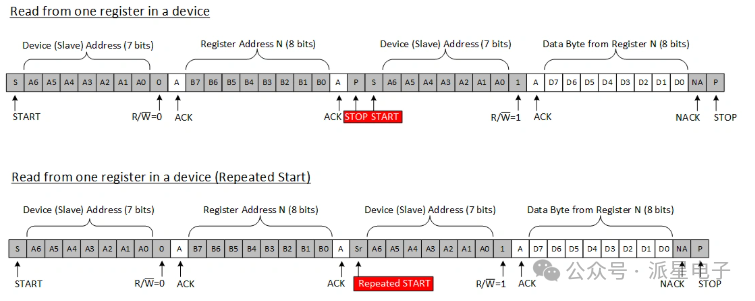
The I2C single-byte read timing is slightly more complex than the write timing, and the read timing is divided into four steps: the first step is to send the device address, the second step is to send the register address to be read, the third step is to send the device address again, and the final step is for the I2C slave device to output the value of the register to be read. Let’s take a closer look at this step.
1. The master sends the start signal.
2. The master sends the I2C slave device address to be read.
3. Read/write control bit, since data is being sent to the I2C slave device, it is a write signal 0.
4. ACK response signal sent by the slave.
5. Resend START signal.
6. The master sends the register address to be read.
7. ACK response signal sent by the slave.
8. Resend START signal.
9. Resend the I2C slave device address to be read.
10. Read/write control bit, here is the read signal 1, indicating that the next step is to read data from the I2C slave device.
11. ACK response signal sent by the slave.
12. The data read from the I2C device.
13. The master sends a NACK signal, indicating that the read is complete, and no further ACK signal is needed from the slave.
14. The master sends a STOP signal, stopping I2C communication.
-Conclusion-
Here are three thought-provoking questions:
-
How to choose the pull-up resistor for I2C? What is it related to?
-
How many devices can be connected on the same I2C bus, and what is it related to?
-
How to solve the overshoot phenomenon of SDA or SCL in IIC?
This content is a systematic summary of I2C bus technology. If you wish to go beyond the application level and deeply understand every detail of the protocol and electrical specifications from the design source, referring to the original official standard document published by NXP is an indispensable step. To facilitate everyone’s learning, we provide access to this authoritative document, and you are welcome to join the group for discussion.
Thank you for reading, and I hope my experience can help you avoid detours.
Exploration by oneself is always slow. True breakthroughs often come from deep exchanges and collisions of ideas with peers. Long press and recognize the following QR code to join the technical group, where ideas can be exchanged, information shared, and progress made together, witnessing each other’s growth.