Recently, I used a SiC MOSFET to create a 200W power supply, and the debugging of the power section went relatively smoothly, achieving a full-load efficiency of 93.3%. However, I encountered issues while debugging the control board.
This control board is mainly used to set reference values for voltage and current in the power section, communicate with the host computer, display status, diagnose faults, and trigger alarms. These functions should have been straightforward, but I stumbled at the reference voltage stage.
The MCU used is the Eastsoft ES32F3663, which features an ARM Cortex-M3 core, a maximum clock frequency of 72MHz, 64KB of FLASH, and 16KB of SRAM, with an operating temperature range of -40°C to 85°C. In terms of peripherals, it is similar to other domestic general-purpose MCUs, supporting 2 channels of 12-bit DAC, 3 analog comparators, and 1 CAN 2.0B interface.
01
Issues with DAC Load Capacity
The power section requires setting reference values for voltage and current to modify the output capability of the power supply, so I used the MCU’s DAC for control, which is slightly cheaper than using PWM. Previously, I had been using the GD32 MCU, and I only modified the minimum system part of the control board circuit, but I ran into problems with the DAC.
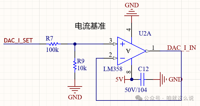
Taking the current reference as an example, the DAC_I_SET signal is directly output from the MCU’s DAC_OUT1. The MCU is powered by 3.3V, and the theoretical output voltage range of the DAC should be 0~3.3V. Thus, DAC_I_IN = DAC_I_SET / 11.
When I set the DAC value to 4095, the measured voltage on DAC_I_SET was only about 900mV, and the operational amplifier output voltage was around 90mV, which was completely off from the expected value.
I then disconnected resistor R7 and tested the DAC_I_SET voltage, which was 3288mV. The DAC output voltage was within the normal range when open-circuited, indicating that the software driver for the DAC was functioning correctly.
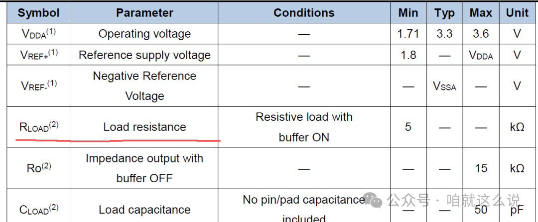
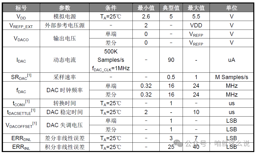
I started checking the specifications and found that the ES32 datasheet did not specify the output load capacity, while the GD32 claimed a load capacity of 5kΩ.
I replaced R7 with a 1M resistor and measured the DAC_I_SET voltage at 3108mV, which was still significantly lowered.
After changing to a 10M resistor, the DAC_I_SET voltage was measured at 3279mV, which, although reduced, was barely acceptable.
GD32 DAC parameter table:
ES32 DAC parameter table:
02
Future Optimization
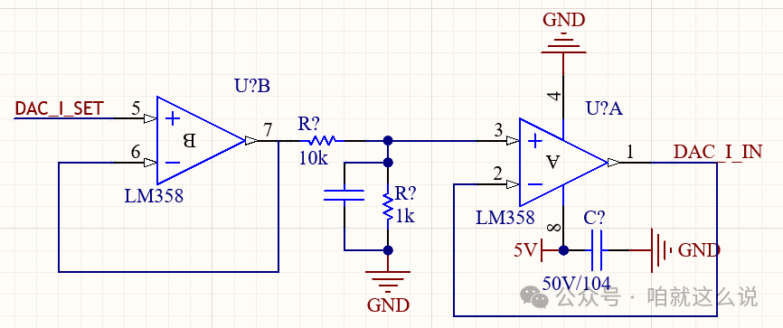
For now, I can only debug and verify the functionality in this state. After verifying the functionality, I will revise the design to connect the DAC output to a voltage follower and then perform signal conditioning.
03
Conclusion
The pitfalls encountered this time were mainly due to not paying attention to the relevant parameters in the datasheet. Additionally, I have reported this issue to the factory’s FAE, hoping they can improve the datasheet soon.
There are still other functions that have not been verified, and I am unsure if there are more pitfalls ahead, but this does not affect my determination to use domestic chips.

Learn to Teach, Earn to Share