In FPGA design, frequency division is often required. For even frequency division, the code is relatively simple; the clock is inverted when the counter reaches half of the division factor, thus completing the even frequency division.For odd frequency division, the approach is slightly more complex. First, two temporary frequency division variables need to be defined: one operates on the rising edge of the clock, and the other on the falling edge. The logic for both operations is that when the counter is less than half of the division factor, it is high; otherwise, it is low. After assigning values to the two temporary frequency division variables, a logical AND operation is performed, and the result is the frequency-divided signal after odd division.Based on the above design concept, FPGA code is designed to achieve a 5-fold division of a 50MHz system clock. The module code is as follows.
//Description: Odd frequency divider module
module odd_div#(    parameter ODD_DIV_COE = 5'D5    )(    input wire clk_50m,    //50MHz clock
    input wire rst_n,    //active low
    output wire clk_div    //clock divide
);
//reg or wire define
reg [4:0] cnt_div;    //frequency division counter
wire [4:0] CNT_DIV_MAX;    //high level time
reg clk_pos;    //rising edge assignment
reg clk_neg;    //falling edge assignment

//main code
//high level time assignment
assign CNT_DIV_MAX = (ODD_DIV_COE >> 1'B1);
//frequency division counter
always @(posedge clk_50m or negedge rst_n) begin
    if(!rst_n)    cnt_div <= 5'd0;
    else if(cnt_div == ODD_DIV_COE - 1'b1)    cnt_div <= 5'd0;
    else    cnt_div <= cnt_div + 1'b1;
end

//clk_pos : rising edge assignment
always @(posedge clk_50m or negedge rst_n) begin
    if(!rst_n)    clk_pos <= 1'b0;
    else if((cnt_div >= 1'b1) && (cnt_div <= CNT_DIV_MAX))    clk_pos <= 1'b1;
    else    clk_pos <= 1'b0;
end

//clk_neg : falling edge assignment
always @(negedge clk_50m or negedge rst_n) begin
    if(!rst_n)    clk_neg <= 1'b0;
    else if((cnt_div >= 1'b1) && (cnt_div <= CNT_DIV_MAX))    clk_neg <= 1'b1;
    else    clk_neg <= 1'b0;
end

//output after odd frequency division
assign clk_div = clk_pos | clk_neg;
endmodule
Write a TestBench simulation for verification, as shown below.
//Description: Frequency division simulation module
`timescale 1ns/1ns
module odd_div_tb();
//define parameter
//reg or wire define
reg clk_50m;
reg rst_n;
wire clk_div;    //clock divide

//main code
initial begin
    clk_50m = 1'b0;
    rst_n <= 1'b0;
    repeat(3) begin
        @(negedge clk_50m);
    end
    rst_n <= 1'b1;
    #1000;    //1us
    $stop;
end

always #10 clk_50m = ~clk_50m;

initial begin
    $display("Test Bench ");
end

//Instantiation
odd_div#(    .ODD_DIV_COE(5'D5)) odd_div_inst(
    .clk_50m(clk_50m),    //50MHz clock
    .rst_n(rst_n),    //active low
    .clk_div(clk_div)    //clock divide
);
endmodule
The waveform is shown in Figure 1, where clk_div is the output result after 5-fold division, and the verification is successful.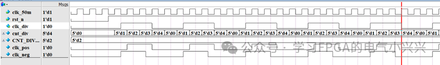 Figure 1: Simulation waveform of the odd frequency divider moduleFor other odd frequency division modules with different division factors, you can change the parameters of the design module and also adjust the width of the counter accordingly.