In a previous article, the author mentioned the embedded power modules from Fraunhofer IZM. The characteristics of this structure are:the module is very thin, and the heat sink is also very thin. However, when the module is fixed to the heat sink, it is evident that the PCB warps.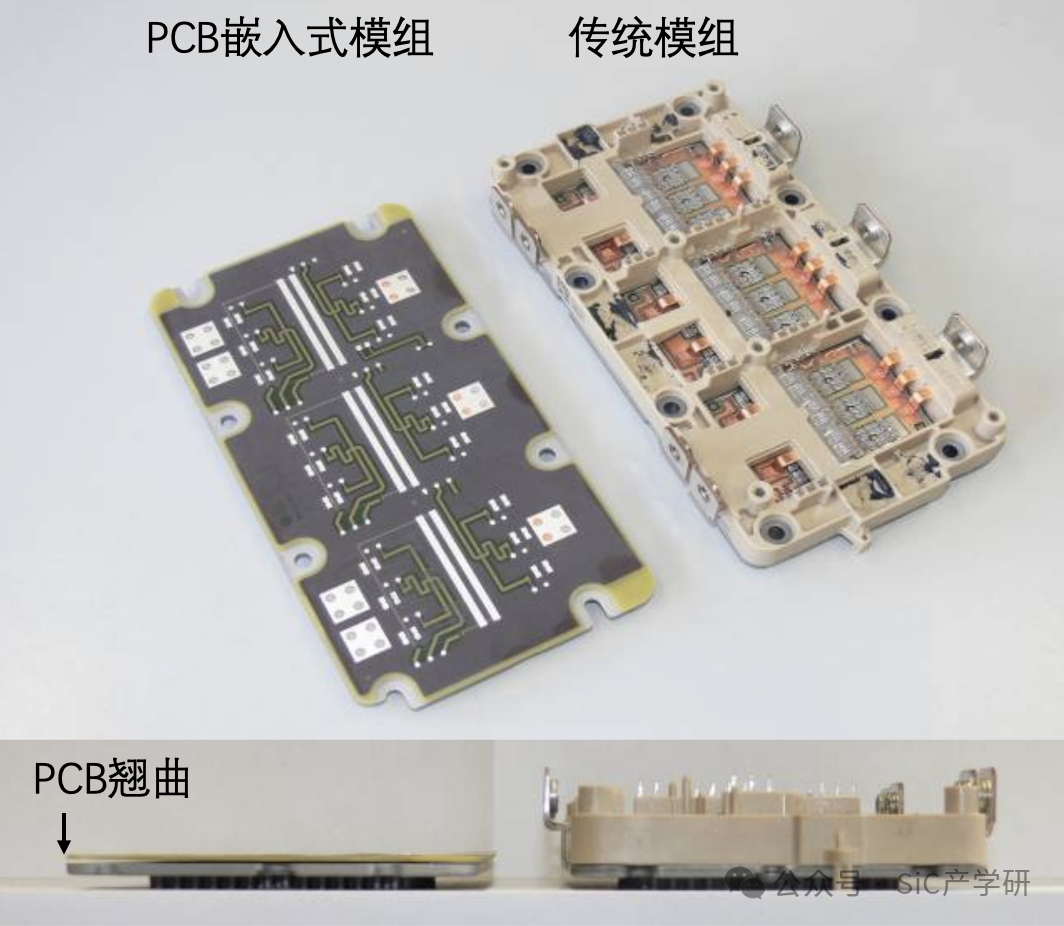
In ordinary PCBs, warping has little effect on heat dissipation—after all, traditional PCBs do not rely on heat sinks and do not involve liquid cooling structures. However, when high-power devices like SiC are embedded in the PCB, the situation is completely different: poor contact caused by warping can significantly increase the temperature of the devices, which is fatal for high-power chips.
The thermal density of power chips is extremely high, and the heat generated must be dissipated quickly and evenly. Once a small gap occurs between the heat sink and the PCB due to warping, the thermal resistance can increase exponentially, potentially leading to local hotspots, triggering thermal runaway, or accelerating aging.
Therefore,the design of embedded power modules in PCBs is not just about designing the PCB itself. The heat sink must also be taken into account to truly ensure the reliability of the embedded module under actual working conditions.
Recently, the author read a research article from the Toyota North America Research Center. Although the article mainly presents simulation results, the ideas proposed regarding the overall structural design of “PCB embedded power modules + heat sinks” are still highly valuable for reference. These analyses have greatly inspired the author’s current thoughts, so the key content is summarized and shared here.
The article mainly introduces the following four structural designs.
The images below are from the original text, and the explanatory text is organized and evaluated by the author based on personal understanding, and does not represent the views of the original author. For the original text, please visit the link at the end.
Structure 1: Embedded module → Thermal paste → Ceramic insulating substrate → Thermal paste → Heat sink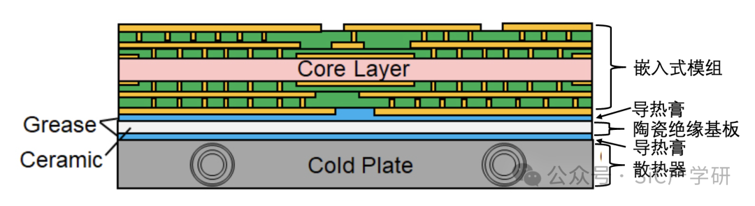
In Structure 1, the heat generated by the embedded PCB module is conducted out sequentially through thermal paste → ceramic insulating substrate → thermal paste → heat sink. Since the embedded module itself does not have an insulating layer, a layer of ceramic insulating substrate must be added between the module and the heat sink.
Thermal paste is inexpensive and, due to its toothpaste-like fluidity, can effectively fill uneven surface areas, achieving very low contact thermal resistance.
However, this advantage is contingent upon—the PCB embedded module not exhibiting significant warping.
Thermal paste does not have a “bonding” function; if warping occurs, as seen in the previous Fraunhofer IZM case, causing the PCB to partially lose contact with the heat sink, the heat dissipation path will immediately fail, equivalent to having no heat sink. For power chips, this almost means “it is impossible for the board not to explode”.
In reality:it is almost impossible for general embedded PCB modules not to warp, so this structure has significant limitations in practical applications. Of course, external fixtures can be used to forcibly compress the PCB against the heat sink to maintain contact.
For example, in the previous article about PCB embedded modules, the author mentioned the Virginia Tech design case:
The thermal resistance of this design is very low, only 0.8 K/W from the chip to the heat sink, but this requires the use of the clamp tip fixture shown below to firmly press the PCB against the heat sink to ensure a sufficiently low thermal resistance path.
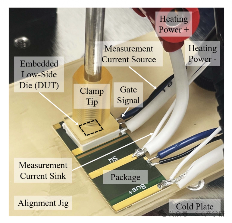
However, doing so completely loses the greatest advantage of the Fraunhofer IZM design compared to traditional modules—“thinness”.
When a large area relies on mechanical structures to compress the module against the heat sink to ensure good contact, the long-term reliability of the design itself becomes a challenge. After all, designs that maintain contact through external forces may experience degradation of contact surfaces under thermal cycling, vibration, and material aging.
Structure 2: Embedded module → Solder → Ceramic insulating substrate → Solder → Heat sink
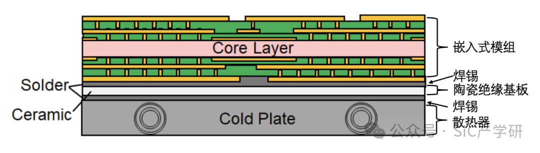
In Structure 2, the heat generated by the embedded PCB module is conducted out sequentially through the solder layer → ceramic insulating substrate → solder layer → heat sink. Similar to Structure 1, but the thermal paste has been replaced with a solder layer.
The thermal conductivity of solder is typically around 50–60 W/m·K, while common thermal pastes usually only range from 2–10 W/m·K. Therefore, Structure 2 has a significant advantage in heat dissipation performance compared to Structure 1.
Additionally, the solder layer has “bonding capability”. Even if the PCB itself has some warping, it can directly bond through the solder layer without needing to rely on fixtures to compress it like in Structure 1. This allows the overall structure to maintain its thin and compact advantages.
So, does this structure have no drawbacks? The main issue is—stress.
Although the PCB is fixed to the heat sink after soldering, the PCB still has an inherent tendency to “warp”. When the structure forcibly suppresses this warping, significant mechanical stress will be generated within the PCB and the solder layer. Additionally, power chips are inherently fragile and do not toleratehigh stress.
Therefore, this structure poses a significant challenge to the long-term reliability of the chip structure; at the same time, it also places higher demands on the fatigue life and reliability of the solder layer.
Structure 3: Embedded module (including insulating resin layer) → Solder → Heat sink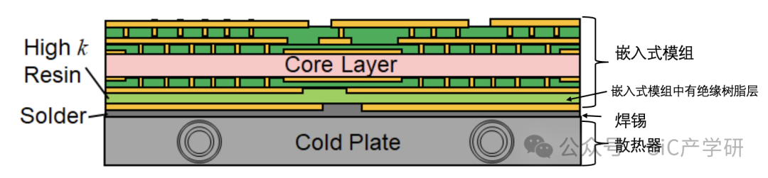
In Structure 3, the ceramic insulating substrate from Structures 1 and 2 is omitted, and a layer of insulating resin layer is added inside the PCB to achieve insulation. At this point, the heat conduction path of the embedded PCB module is: insulating resin layer → solder layer → heat sink.
Since the insulation function is already achieved within the PCB, this structure is simpler and has a higher integration level than the previous two.
However, its challenges are also very apparent: the thermal conductivity of insulating resin layers is typically poor.
Especially when the power module needs to meet 1200 V voltage resistance, the insulating layer must be thick enough to ensure electrical safety, which further increases thermal resistance, making heat dissipation more difficult.
Additionally, similar to Structure 2, since a solder layer is used for “forced fixation”, the PCB’s tendency to warp will still generate significant internal stress. Therefore, stress control and long-term reliability issues remain.
Structure 4: Embedded module → Heat-dissipating insulating resin layer → Heat sink
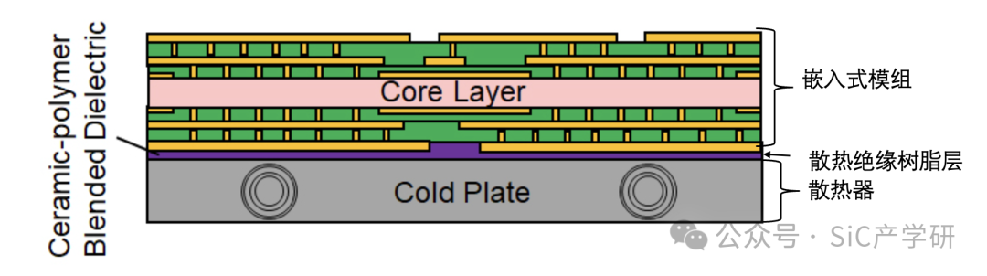
Structure 4 is the simplest of the four schemes. A resin material that combines heat dissipation performance, insulation capability, and bonding ability is used between the module and the heat sink (the article does not provide details, but it is likely a system of epoxy resin + ceramic filler).
The insulation, heat dissipation, and bonding functions are achieved by the same resin layer, significantly simplifying the overall structure.
Using a resin layer to perform both insulation and heat dissipation roles, compared to the insulating resin layer inside the PCB in Structure 3, the resin layer in Structure 4 can achieve better thermal conductivity. This is due to the type and ratio of fillers used, as such materials on the market can achieve a thermal conductivity of 5–8 W/m·K.
Of course, this structure still relies on the resin layer to “force fix” the PCB, so stress issues remain. However, compared to the solder layer, resin materials are relatively “softer”, which can significantly reduce stress concentration and be more favorable for the reliability of the chip and structure.
The article also mentions asymmetric PCB structures solutions, but their structural design ideas with the heat sink are similar to the above several, so they will not be elaborated here.
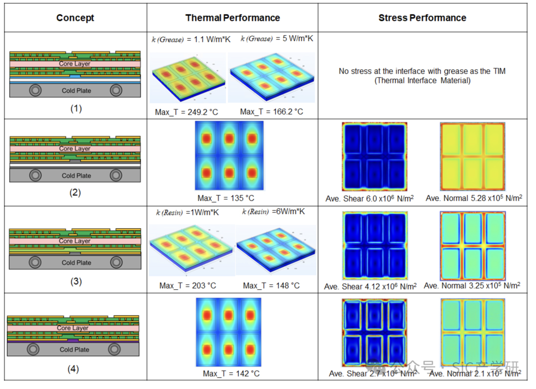
The article simulated the chip temperature and stress under the four structures, and the results were consistent with the previous analysis.
-
Structure 1: Using thermal paste to fix the PCB to the heat sink
Thermal paste does not introduce additional stress, which is its advantage. However, due to its lower thermal conductivity, the chip temperature is relatively high.
-
Structure 2: Using solder layer to fix the PCB to the heat sink
The chip temperature is the lowest, making it the best heat dissipation structure. However, the stress is also the highest, putting the most pressure on reliability.
-
Structure 3: Using the insulating resin layer inside the PCB
Compared to Structure 2, the chip temperature rises slightly, but the stress is also reduced.
-
Structure 4: Using heat-dissipating insulating resin layer
Although the chip temperature is higher than Structure 2, it is better than thermal paste (Structure 1) and the PCB insulating resin layer (Structure 3). More importantly, since there is no solder layer, the stress is significantly reduced, making it the least stressful solution.
Summary 🌟🌟🌟
This paper, although not lengthy, presents ideas regarding the overall structural design of “PCB embedded power modules + heat sinks” that are still very worthy of reference. The heat dissipation design of embedded PCB power modules is closely intertwined with factors such as PCB routing, RDL (redistribution layer) reliability, and insulation design.
After all the hard work in designing the routing and structure, achieving parasitic inductance close to 0 nH, only to find that when combined with the heat sink, heat cannot dissipate, and the RDL repeatedly breaks… ultimately having to redesign the PCB and adjust the routing. It’s a hassle to think about.
Embedded PCB modules essentially blur the boundaries between electricity, heat, insulation, and stress, meaning all factors must be considered together as a whole, rather than optimizing just one.
The Toyota paper was published in 2023, and based on the research pace, the experiments likely began 2-3 years prior. Now, nearly 5 years later, there has been no news of Toyota mass-producing embedded PCB modules. This likely indicates that finding the optimal balance between electricity, heat, insulation, and stress in overall structural optimization is indeed quite challenging.
Recently, there have been many messages online about embedded power modules, but most showcase physical PCB units or 3D models of PCB + heat sinks, while the overall structure of PCB + heat sink is still relatively rare.
Hopefully, in the near future, the industry will see more mature overall solutions implemented, and I look forward to everyone’s joint efforts 💪
Original text 🔗: https://ieeexplore.ieee.org/document/10213601
A small request 


If this content is helpful to you, please like, share, bookmark, and follow this account🙏Your support is my greatest motivation for continued writing and sharing 💪Feel free to exchange ideas in the comments section, let’s discuss and think together Please also respect original content; if you need to share it on other platforms, please contact and indicate the source. Recently, I have seen some unauthorized reposts on Xiaohongshu without proper attribution. Respecting originality allows knowledge to flow for a long time🙏