As an embedded engineer, you should know about download debuggers, but do you really understand the meanings and differences between the SWD and JTAG interfaces?
What is a Download Debugger
In simple terms, a download debugger is a device that converts commands sent from a PC (for example, via USB protocol) into a language understood by the MCU (responsible for the internal peripherals of the MCU), such as the SWD or JTAG protocol, to load code and precisely control execution.
Debugger Protocol Standards
In simple terms, a standard is a set of rules and protocols that every participant in a specific industry agrees to follow and implement.
2. The Chaos of Debugger Protocols
Before protocols like SWD and JTAG emerged, there was chaos among debuggers and their protocols, with each MCU manufacturer proposing its proprietary methods to load code onto their MCUs. Every time a manufacturer released a new MCU, embedded software engineers had to understand its proprietary protocol to load code onto the microcontroller.
Moreover, debug adapters were expensive because manufacturers did not have competitors that could match their protocols, as the protocols were proprietary. Another reason for their high cost was due to a lack of volume, as they could only sell debug adapters to companies (engineers) using the MCUs they manufactured.
The different protocols also led to increased development costs. For example, if you have four different chips from four different manufacturers on the board you are designing and wish to perform some automated testing to improve production efficiency, you would need to create a super complex production code that accommodates the complexity, and install four different debuggers at the test points on the board, thus increasing costs, production time, and programming time.
3. Establishing Protocols
The various download debugging differences can lead to several issues:
-
Investing more time in learning
-
Increasing costs for downloading debugging
-
Generating inefficient testing
To address this issue, engineers from major MCU manufacturers and producers have formulated some standard protocols for debugging.
JTAG: Joint Test Action Group, which stands for the Joint Test Action Group.
This group began discussions in the late 1980s and officially released documentation interpreting the IEEE standard in 1990. (IEEE stands for the Institute of Electrical and Electronics Engineers, an international organization that publishes all standards, such as WiFi, Bluetooth, etc.). The protocol they proposed was recorded in IEEE 1149.1 in 1990. The document has been revised and improved, and as of the writing of this article, the latest standard is IEEE 1149.7.
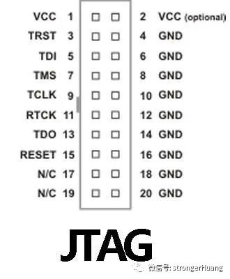
JTAG basically has 5 pins:
TDI: Test Data In. Serial input pin
TDO: Test Data Out, serial output pin
TCK: Test Clock, clock pin
TMS: Test Mode Select, mode select (control signal) pin
TRST: Test Reset, reset pin
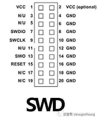
SWD: Serial Wire Debug, representing Serial Wire Debugging, is a protocol designed by ARM for programming and debugging its microcontrollers.
Since SWD is specifically designed for programming and debugging, it has many special features that are often unavailable elsewhere, such as sending debugging information to a computer through IO lines. Additionally, because it is manufactured specifically for use in ARM devices, the performance of SWD is often the best in its class!
SWDIO: Serial Wire Data Input Output, serial data input output pin
SWCLK: Serial Wire Clock, serial wire clock pin
Various Differences Between SWD and JTAG
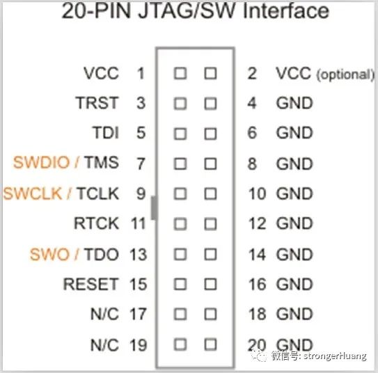
There are many MCUs and debug adapters on the market that are compatible with both SWD and JTAG protocols. They typically achieve download and debugging functions through a set of download debug pins that are internally multiplexed to the SWD peripherals and JTAG peripherals.
The pins of SWD can be multiplexed with JTAG pins under certain conditions. Currently, there are many connectors for JTAG and SWD, such as the 20-pin connector:
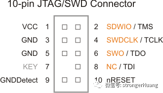
Of course, there are also 10-pin connectors:
2. Advantages of SWD and JTAG
Advantages of the SWD Protocol:
-
Uses fewer pins, only requiring the SWDIO and SWCLK pins
-
SWD has special features, such as printing debugging information through its I/O lines
-
Compared to JTAG, SWD has better overall performance in terms of speed
Advantages of the JTAG Protocol:
-
JTAG is not limited to ARM chips; it also supports chips outside of ARM, such as the well-known MSP430
-
JTAG has more versatility, used for programming, debugging, and production testing
-
JTAG is an independent group that evolves with the development of the protocol
3. When to Choose SWD Over JTAG
-
If your schematic/circuit board design is simple enough to test without JTAG functionality
-
If debugging performance is more important than production testing, and your device focuses on research rather than mass production!
-
If the MCU has size limitations, SWD can save space
-
If your hardware design is too complex, and the MCU has no extra 2 pins
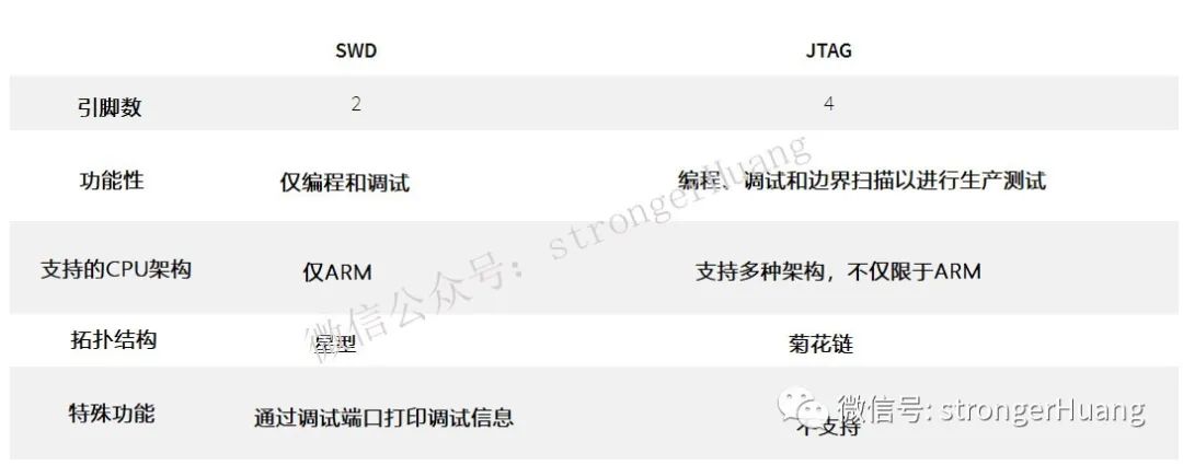
Summary: SWD / JTAG Comparison
Below is a summary in one diagram:

There are many considerations for including C language header files!
Can a PCB carry a current of 100A? Tips for setting up high current paths
Byte knowledge that every microcontroller learner must know
Summary of data transmission and reception methods for STM32 serial ports!
The “ground” in switch-mode power supplies and how to “ground” it

Click “Read Original” to see more shares, and feel free to share, bookmark, like, and view.