Follow+Star PublicAccount, don’t miss exciting content
WeChat Public Account | Embedded Column
The mainstream download interfaces for microcontrollers based on the Cortex-M core are JTAG and SWD.
Differences Between SWD and JTAG Pins:
-
TDI: Test Data In. Serial input pin
-
TDO: Test Data Out, serial output pin
-
TCK: Test Clock, clock pin
-
TMS: Test Mode Select, mode select (control signal) pin
-
TRST: Test Reset, reset pin
-
SWDIO: Serial Wire Data Input Output, serial data input output pin
-
SWCLK: Serial Wire Clock, serial wire clock pin
SWD only requires two wires (SWCLK and SWDIO). In cases of limited PCB layout and tight pin resources, SWD is a good choice.
SWD: Serial Wire Debug, represents serial wire debugging, is a protocol designed by ARM for programming and debugging its microcontrollers.
There are many downloaders on the market that support the SWD debugging interface, such as:ST-Link, J-Link, e-Link, GD-Link and most of the downloaders used for Cortex-M core processors support it.
For SWDIO, it is a bidirectional (input-output) data pin, and a pull-up must be applied to the circuit board (ARM recommends using 100 K).
Each time the direction of SWDIO changes in the protocol, a transition time is inserted, during which the line is not driven by either the host or the target. By default, this transition time is one bit time, but it can be adjusted by configuring the SWCLK frequency.
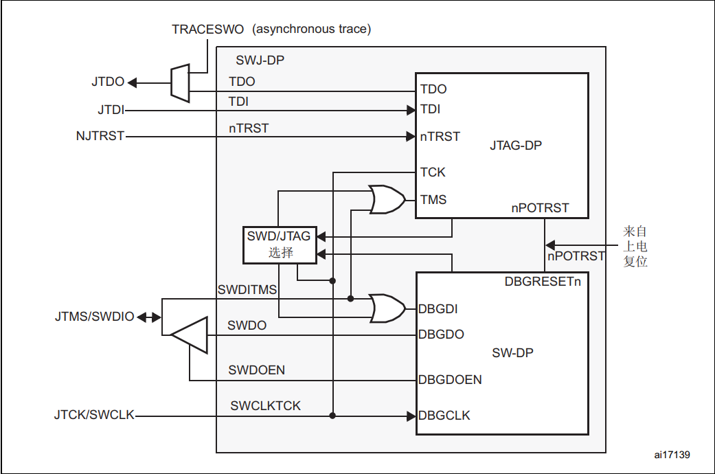
Common Cortex-M core processors integrateSWD and JTAG debug ports, in the SWJ-DP, the 2 JTAG pins of SW-DP are multiplexed with some of the 5 JTAG pins of JTAG-DP.
Switching Mechanism Between JTAG and SWD:
The default debug interface is the JTAG interface. If the debugging tool wants to switch to SW-DP, it must provide a dedicated JTAG sequence on TMS/TCK (mapped to SWDIO and SWCLK) to disable JTAG-DP and enable SW-DP. This allows SWDP to be activated using only the SWCLK and SWDIO pins.
1. Output TMS (SWDIO) = 1 signal for more than 50 TCK cycles
2. Output 16 TMS (SWDIO) signals 0111100111100111 (MSB)
3. Output TMS (SWDIO) = 1 signal for more than 50 TCK cycles
Each sequence consists of three phases:
-
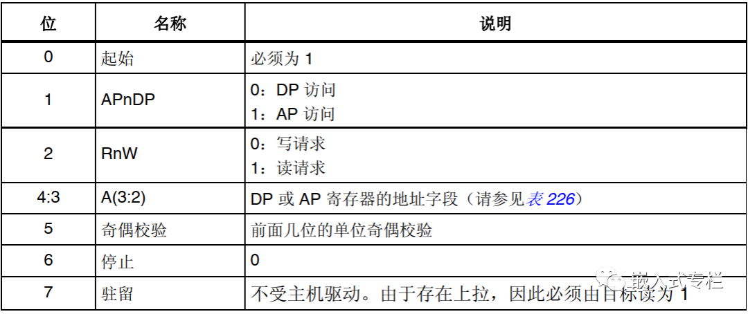
The host sends a data packet request (8 bits)
-
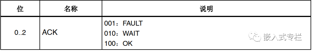
The target sends an acknowledgment response (3 bits)
-
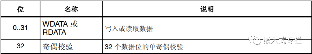
The host or target sends the data transfer phase (33 bits)
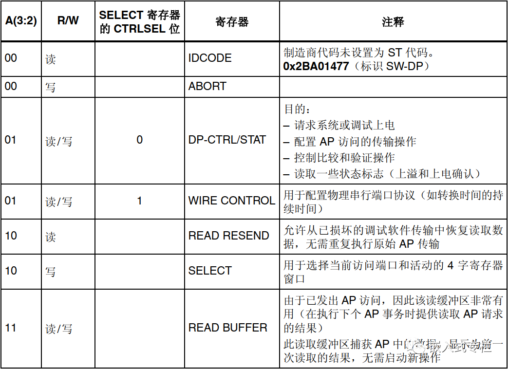
Data Packet Request (8 bits):
This is similar to bit operations of registers; some underlying principles are similar toordinary communication protocols.
The SW-DP state machine has an internal ID code to identify SW-DP, which mainly includes states: reset, idle state, ID code, etc.
-
After power-on reset, when DP switches from JTAG to SWD, or when the line is high for more than 50 cycles, the SW-DP state machine is in the reset state.
-
If the line is low for at least two cycles after the reset state, the SW-DP state machine is in the idle state.
-
After the reset state, the state machine must first enter the idle state and then perform a read access to the DP-SW ID CODE register. Otherwise, the target will issue a FAULT acknowledgment response on another transaction.
For more details about the SW-DP state machine, refer tosome manuals related to Cortex-M.
SWD is similar to ordinary peripherals and has a kind of register. The programming operations (read/write) performed by developers are actually operations on the corresponding registers.
This concludes the introduction to the underlying aspects of SWD. For more details, please refer toCortex-M core manuals.
———— END ————
● Column “Embedded Tools”
● Column “Embedded Development”
● Column “Keil Tutorial”
● Selected Tutorials from Embedded Column
Follow the public account reply “Join Group” to join the technical exchange group according to the rules, reply “1024” to see more content.

Click “Read Original” to see more shares.